
Chapter Four The Processor: Datapath and Control
E N D
Presentation Transcript
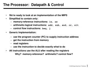
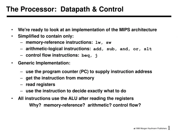
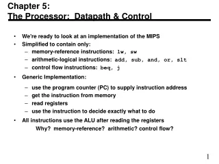
4.1 Introduction A Basic MIPS Implementation • We're ready to look at an implementation of the MIPS • Simplified to contain only: • memory-reference instructions: lw, sw • arithmetic-logical instructions: add, sub, and, or, slt • control flow instructions: beq, j • Generic Implementation: • use the program counter (PC) to supply instruction address • get the instruction from memory • read registers • use the instruction to decide exactly what to do • All instructions use the ALU after reading the registers Why? memory-reference? arithmetic? control flow?
An Overview of the Implementation • For most instructions: fetch instruction, fetch operands, execute, store. • An abstract view of the implementation of the MIPS subset showing the major functional units and the major connections between them • Missing Multiplexers, and some Control lines for read and write.
Continue • The basic implementation of the MIPS subset including the necessary multiplexers and control lines. • Single-cycle datapath (long cycle for every instruction. • Multiple clock cycles for each instruction>
4.2 Logic Design Conventions • Combinational elements & State elements State elements • Unclocked vs. Clocked • Clocks used in synchronous logic • when should an element that contains state be updated?
Clocking Methodology • An edge triggered methodology • Typical execution: • read contents of some state elements, • send values through some combinational logic • write results to one or more state elements
We need functional units (datapath elements) for: Fetching instructions and incrementing the PC. Execute arithmetic-logical instructions: add, sub, and, or, and slt Execute memory-reference instructions: lw, sw Execute branch/jump instructions: beq, j Fetching instructions and incrementing the PC. 4.3 Building a Datapath
Execute arithmetic-logical instructions: add, sub, and, or, and slt add $t1, $t2, $t3 # t1 = t2 + t3 Continue
Execute memory-reference instructions: lw, sw lw $t1, offset_value($t2) sw $t1, offset_value($t2) Continue
Execute branch/jump instructions: beq, j beq $t1, $t2, offset
Creating a Single Datapath • Sharing datapath elements Example: Show how to built a datapath for arithmetic-logical and memory reference instructions.
Continue Now we con combine all the pieces to make a simple datapath for the MIPS architecture:
4.4 A Simple Implementation Scheme The ALU Control
Why a Single-Cycle Implementation Is Not Used Today Example: Performance of Single-Cycle Machines Calculate cycle time assuming negligible delays except: • memory (200ps), • ALU and adders (100ps), • register file access (50ps) Which of the following implementation would be faster: • When every instruction operates in 1 clock cycle of fixes length. • When every instruction executes in 1 clock cycle using a variable-length clock. To compare the performance, assume the following instruction mix: 25% loads 10% stores 45% ALU instructions 15% branches, and 5% jumps
Continue CPU clock cycle (option 1) = 600 ps. CPU clock cycle (option 2) = 400 45% + 60025% + 550 10% + 350 15% + 2005% = 447.5 ps. Performance ratio = • memory (200ps), • ALU and adders (100ps), • register file access (50ps) • 45% ALU instructions 25% loads • 10% stores • 15% branches, and • 5% jumps
4.5 A Multicycle Implementation • A single memory unit is used for both instructions and data. • There is a single ALU, rather than an ALU and two adders. • One or more registers are added after every major functional unit.
Continue Replacing the three ALUs of the single-cycle by a single ALU means that the single ALU must accommodate all the inputs that used to go to the three different ALUs.
Continue Control signals: • The programmer-visible state units (PC, Memory, Register file) and IR write Memory Read • ALU control: same as single cycle • Multiplexor single/two control lines
Continue PC write control signal: PCWrite : PC+4 and jump PCWriteCond : beq Three possible sources for the PC: • PC+4 • ALUOut : address of the beq • Address for jump ( j )
Breaking the Instruction Execution into Clock Cycles • Instruction fetch step • IR <= Memory[PC]; • PC <= PC + 4; IR <= Memory[PC]; MemRead IRWrite IorD = 0 ------------------------------- PC <= PC + 4; ALUSrcA= 0 ALUSrcB= 01 ALUOp = 00 (for add) PCSource = 00 PCWrite The increment of the PC and instruction memory access can occur in parallel, how?
Breaking the Instruction Execution into Clock Cycles • Instruction decode and register fetch step • Actions that are either applicable to all instructions • Or are not harmful A <= Reg[IR[25:21]]; B <= Reg[IR[20:16]]; ALUOut <= PC + (sign-extend(IR[15-0] << 2 );
Instruction decode and register fetch step • A <= Reg[IR[25:21]]; • B <= Reg[IR[20:16]]; • ALUOut <= PC + (sign-extend(IR[15-0] << 2 ); A <= Reg[IR[25:21]]; B <= Reg[IR[20:16]]; Since A and B are overwritten on every cycle Done ------------------------------------------ ALUOut <= PC + (sign-extend(IR[15-0]<<2); This requires: ALUSrcA 0 ALUSrcB 11 ALUOp 00 (for add) branch target address will be stored in ALUOut. The register file access and computation of branch target occur in parallel.
Breaking the Instruction Execution into Clock Cycles • Execution, memory address computation, or branch completion Memory reference: ALUOut <= A + sign-extend(IR[15:0]); Arithmetic-logical instruction: ALUOut <= A op B; Branch: if (A == B) PC <= ALUOut; Jump: PC <= { PC[31:28], (IR[25:0], 2’b00) };
3. Execution, memory address computation, or branch completion Memory reference: ALUOut <= A + sign-extend(IR[15:0]); ALUSrcA= 1 && ALUSrcB = 10 ALUOp = 00 Arithmetic-logical instruction: ALUOut <= A op B; ALUSrcA= 1 && ALUSrcB = 00 ALUOp = 10 Branch: if (A == B) PC <= ALUOut; ALUSrcA= 1 && ALUSrcB = 00 ALUOp = 01 (for subtraction) PCSource= 01 PCWriteCond Jump: PC <= { PC[31:28], (IR[25:0],2’b00) }; PCSource = 10 PCWrite
Breaking the Instruction Execution into Clock Cycles • Memory access or R-type instruction completion step Memory reference: MDR <= Memory [ALUOut]; MemRead or IorD=1 Memory [ALUOut] <= B; MemWrite Arithmetic-logical instruction (R-type): Reg[IR[15:11]] <= ALUOut; RegDst=1RegWrite MemtoReg=0 • Memory read completion step Load: Reg[IR[20:16]] <= MDR; MemtoReg=1RegWriteRegDst=0
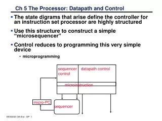
Defining the Control Two different techniques to design the control: • Finite state machine • Microprogramming Example: CPI in a Multicycle CPU Using the SPECINT2000 instruction mix, which is: 25% load, 10% store, 11% branches, 2% jumps, and 52% ALU. What is the CPI, assuming that each state in the multicycle CPU requires 1 clock cycle? Answer: The number of clock cycles for each instruction class is the following: • Load: 5 • Stores: 4 • ALU instruction: 4 • Branches: 3 • Jumps: 3
Example Continue The CPI is given by the following: is simply the instruction frequency for the instruction class i. We can therefore substitute to obtain: CPI = 0.255 + 0.104 + 0.524 + 0.113 + 0.023 = 4.12 This CPI is better than the worst-case CPI of 5.0 when all instructions take the same number of clock cycles.
Continue • Finite state machine controllers are typically implemented using a block of combinational logic and a register to hold the current state.
4.6 Exceptions • Exceptions • Interrupts
How Exception Are Handled To communicate the reason for an exception: • a status register ( called the Cause register) • vectored interrupts
How Control Checks for Exception Assume two possible exceptions: • Undefined instruction • Arithmetic overflow
Continue The multicycle datapath with the addition needed to implement exceptions
Continue The finite state machine with the additions to handle exception detection