Imaging and modeling diffusion to defects in GaAs
10 likes | 227 Vues
Imaging and modeling diffusion to defects in GaAs Mac Read and Tim Gfroerer, Davidson College, Davidson, NC Mark Wanlass, National Renewable Energy Lab, Golden, CO. Abstract. Motivation. Diffusion to Defect Model.

Imaging and modeling diffusion to defects in GaAs
E N D
Presentation Transcript
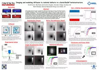
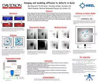
Imaging and modeling diffusion to defects in GaAs Mac Read and Tim Gfroerer, Davidson College, Davidson, NC Mark Wanlass, National Renewable Energy Lab, Golden, CO Abstract Motivation Diffusion to Defect Model Defect-related electron-hole recombination impairs the performance of many semiconductor devices. At high excitation, the density of electrons and holes is higher, so they encounter each other more frequently. Early encounters reduce the average lifetime and diffusion distance so the carriers are less likely to reach defects. We observe native defects in a GaAs epilayer where the area of the defect-dominated region depends strongly on excitation intensity. We model the behavior with a simulation that allows for lifetime-limited diffusion of carriers, and we report good qualitative agreement between the experimental and simulated images. Defect-related Recombination Radiative Recombination The radiative efficiency is the ratio of the radiative and total recombination rates: Conduction Band Conduction Band - - The defect-related recombination rate scales linearly with the carrier density n, while the radiative rate is proportional to n2. A and B are coefficients that set the magnitude of the defect and radiative rates, respectively. Defect Level ENERGY HEAT HEAT LIGHT + + Valence Band Valence Band Experimental Images Modeling Results Electrons can recombine with holes in semiconductors by hopping through localized defect states and releasing heat. This defect-related trapping and recombination process is a loss mechanism that reduces the efficiency of many semiconductor devices. - - Diffusion - Low-excitation High-excitation + - + d - - y D y D + + + - d - Low density High density A=4.2*107 cm3/s A=8.2*104 cm3/s x x D Defect - Electron + Hole The carrier lifetime is determined by how long it takes an electron to find a suitable hole for recombination. At low excitation density, electrons are more likely to encounter a defect before a hole, allowing for defect-related trapping and recombination. At high excitation, the electrons and holes don’t live as long, reducing the diffusion length d and the probability of reaching a defect before radiative recombination occurs. We model the defect as an isolated pixel with an augmented defect (A) coefficient. Diffusion to this pixel reduces the carrier density n near the defect, and since the brightness is proportional to the radiative rate Bn2, the adjacent region appears darker. Using the model and algorithm shown to the right, we obtain the theoretical images above. These images, with A=4.2*107 cm3/s (defect pixel) and A=8.2*104 cm3/s (non-defect pixels), produced the lowest error. Photoluminescence images are obtained from an undoped GaAs/GaInP heterosturcture. The excitation intensity-dependent images shown above center on a native defect in the thin, passivated GaAs layer. The Algorithm Experimental Setup The algorithm to find steady state carrier densities (n) follows a simple rate equation including generation, recombination, and Laplacian diffusion: Conclusions • Even for high-quality semiconductor materials with few defects, diffusion can lead to significant defect recombination at low excitation intensity. • At low density, carriers diffuse more readily to defective regions rather than recombining radiatively, producing larger effective “dead” areas. • If the defect constant A is non-uniform throughout the sample, diffusion will contribute to a reduction in net efficiency. • The behavior can be modeled by assigning a larger A coefficient to the defect and allowing diffusion to control the density of carriers. • Although not shown here, our model also appears to be qualitatively consistent with preliminary temperature-dependent measurements. Where Eex is the photon energy, d is the layer thickness, and Dn is the diffusion coefficient for electrons in GaAs. • The different A coefficients produce different recombination rates in the defect and non-defect pixels, which yield different carrier densities. • We use Laplacian diffusion to determine the flux between adjacent pixels during each time step and then calculate new carrier densities. • We allow the diffusion process to continue until the average lifetime of the generated carriers is reached. • Then we adjust the defect and non-defect A coefficients to minimize the error between model and experiment. Acknowledgment We thank Jeff Carapella for growing the test structures and the Donors of the American Chemical Society – Petroleum Research Fund for supporting this work. Carrier density is reduced by diffusion to the defect