Download
1 / 1
30 likes | 202 Vues
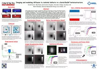
Conduction Band. Ec. Energy. Ev. Valence Band. Imaging and modeling diffusion to isolated defects in a GaAs/GaInP heterostructure Tim Gfroerer, Mac Read, and Caroline Vaughan, Davidson College, Davidson, NC Mark Wanlass, National Renewable Energy Lab, Golden, CO. Motivation.

E N D
Conduction Band Ec Energy Ev Valence Band Imaging and modeling diffusion to isolated defects in a GaAs/GaInP heterostructure Tim Gfroerer, Mac Read, and Caroline Vaughan, Davidson College, Davidson, NC Mark Wanlass, National Renewable Energy Lab, Golden, CO Motivation Yes! A Better Recombination Model Abstract Defect-related Recombination Radiative Recombination Conduction Band Conduction Band Defect-related electron-hole pair recombination impairs the performance of many semiconductor devices. In photoluminescence images, defective regions appear dark because carriers are more likely to recombine nonradiatively. We use photoluminescence imaging to observe isolated defects in a GaAs/GaInP heterostructure. We find that the area of the defect-darkened region depends strongly on the photoexcitation intensity. With increasing excitation, the density of electrons and holes increases, so they are more likely to encounter each other and recombine radiatively before reaching the defect. We model the behavior with a computer simulation that allows for lifetime-limited Laplacian diffusion of carriers, and we report good qualitative agreement between the experimental and simulated images. We are currently developing a more sophisticated model in hopes of achieving better quantitative agreement. - - Defect Level ENERGY HEAT LIGHT HEAT + + 100 µm 100 µm 100 µm 100 µm Valence Band Valence Band Nonequilibrium electrons can recombine with holes in semiconductors by hopping through localized defect states and releasing heat. This defect-related trapping and recombination process is a loss mechanism that reduces the efficiency of many semiconductor devices. Experimental Images Better Recombination Model? If we assume that all defect levels are concentrated near the center of the bandgap as shown above, then the concentration of non-equilibrium electrons in the conduction band n will equal that of holes in the valence band, and thermal excitation out of the traps can be neglected. These assumptions lead to the defect-related recombination rate An that is used in the panels to the left. 100 µm 100 µm 100 µm 100 µm Diffusion Low-excitation High-excitation + - + d - - y D y D + + + 100 µm 100 µm - d - x x D Defect - Electron + Hole At low excitation density, electrons are more likely to encounter a defect before a hole, allowing for defect-related trapping and recombination. At high excitation, the electrons and holes don’t live as long, reducing the diffusion length d and the probability of reaching a defect before radiative recombination occurs. The new defect-related DOS function shown above fits our radiative efficiency measurements by generating asymmetric band filling. When the electron traps are saturated, the concentration of electrons in the conduction band ne rises sharply with excitation. Since a high concentration of holes np is already present in the valence band, a rapid increase in the radiative rate Bne np occurs. 100 µm 100 µm Photoluminescence images are obtained from an undoped GaAs/GaInP heterostructure. The excitation intensity-dependent images shown above center on an isolated defect in the thin, passivated GaAs layer. If we allow the defect rate coefficient A to vary with excitation, we can reproduce our experimental results. However, variation of A with excitation is non-physical. We need a better model for defect-related recombination. Experimental Setup Conclusions and Future Work Raditative Efficiency Simple Recombination Model • Even for high-quality semiconductor materials with few defects, diffusion can lead to significant defect recombination at low excitation intensity. • At low density, carriers diffuse more readily to defective regions rather than recombining radiatively, producing larger effective “dead” areas. • A defect-related recombination model that allows for an asymmetric distribution of defect levels within the bandgap is needed to account for our experimental results. • To incorporate the new recombination model into our diffusion simulation, we need to understand why/how our radiative efficiency measurements depend on the laser spot size. 100 μm ? Measurements of radiative efficiency (emitted / absorbed light) as a function of photoexcitation. The solid lines are theoretical fits assuming that the rate of defect-related recombination is simply a constant A times the photoexcited carrier density n. Acknowledgments We use a high-sensitivity camera to obtain photoluminescence images over a broad range of laser powers. We can also measure the integrated photoluminescence intensity as a function of photoexcitation. We thank Jeff Carapella for growing the test structures and Adam Topaz for writing the code that identifies good defect-related DOS functions. We also thank the Davidson Research Initiative and the Donors of the American Chemical Society – Petroleum Research Fund for supporting this work. We model the defect as an isolated pixel with an augmented rate of defect-related recombination An. Diffusion to this pixel reduces the carrier density n near the defect, and since brightness is proportional to the radiative rate Bn2, the adjacent region appears darker. This model yields poor agreement between experiment and theory. Radiative efficiency measurements cannot be explained if we assume that the defect-related recombination rate equals An. We need a better model.