Oscillators
Oscillators. OEMIC 이 현 태. Contents. Theory of the Oscillator Push-push Oscillator Frequency Multiplier Oscillator Semi-MMIC Push-push Oscillator Shunt Feedback Oscillator using MEMS Cavity Resonator VCO using Coplanar Waveguide. Oscillator. Introduction.

Oscillators
E N D
Presentation Transcript
Oscillators OEMIC 이 현 태 Kwangwoon University
Contents • Theory of the Oscillator • Push-push Oscillator • Frequency Multiplier Oscillator • Semi-MMIC Push-push Oscillator • Shunt Feedback Oscillator using MEMS Cavity Resonator • VCO using Coplanar Waveguide Kwangwoon University
Oscillator Kwangwoon University
Introduction • - DC power를 AC power로 변환해 주는 에너지 반전 소자 • - 외부에서 별도로 입력 신호를 인가해 주지 않음 • ---> 증폭회로에서 출력의 일부를 입력측에 궤환시킴으로써 발진이 발생 Kwangwoon University
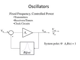
The composed of Oscillator 1. Negative Resistace 2. Resonator 3. Load Kwangwoon University
Type of Resonators 1. Cavity Resonator 2. Planar Microstrip Resonator 3. Dielectric Resonator : DR Kwangwoon University
Cavity Resonator • 1. Waveguide Resonator • 2. Coaxial Resonator • 장 점 • - Isolation 특성이 좋다 • - Power Capability가 크다 • - Q(Quality factor)값이 높다. • - 제작이 용이하다 • - Line Loss 가 적다 • 단 점 • - 부피가 크고 무겁다 • - 집적화가 곤란하다 • - 대역폭이 좁다 Kwangwoon University
Planar Microstrip Resonator • 1. Rectangular Microstrip Resonator • 2. Microstrip Disk Resonator • 3. Microstrip Ring Resonator • 4. Triangular Microstrip Resonator • 5. Hexagonal Microstrip Resonator • 장 점 • - 일반적으로 대역폭이 크다 • 소형이고 집적화가 용이하다 • - 회로구현이 쉽다. • 단 점 • - Line loss가 크다 • - Q값이 적다 • - Isolation 시키기가 어렵다 Kwangwoon University
Dielectric Resonator : DR - Ceramic 재질의 공진기 - 저손실, 온도 안정성, 높은 유전율과 높은 Q (>2000) - 소형, 저가, 간단한 구조 Kwangwoon University
Hair-pin Resonator • Hairpin Resonator의 종류 (a) (b) (c) (a) 일반적인 Hair-pin Resonator (b) 소형화된 Hair-pin Resonator (c) 커플링 라인을 갖는 소형 Hair-pin Resonator Kwangwoon University
Coupling Line 을 갖는 소형 Hair-pin Resonator의 특성 - 평면구조 ---> M(M)IC 프로세스에 적합 - 소 형 - 응용 주파수의 확대 - 주파수 튜닝의 용이성 (커플링 라인의 조절로 가능) Kwangwoon University
Hair-pin Resonator의 Electrical Parameters Zs: Single line의 특성 임피던스 θs : Single line의 전기적 길이 Zpe& Zpo : Parallel line의 우수 및 기수 모드 특성 임피던스 θpeand θpo : Parallel line의 우수 및 기수 모드 전기적 길이 Kwangwoon University
Parallel Coupled Lines andTransmission Lines의 Equivalent Circuits Parallel Coupled Lines A Transmission Line Kwangwoon University
Parallel Coupled Lines andTransmission Linesabout ABCD Matrices: • If Kwangwoon University
Equivalent Circuits방법 • - Open circuit end 구조를 갖는 Parallel Coupled Lines은 공진점에서 even mode • 와 odd mode 를 갖게 됨. • Equivalent Circuits (a) Even mode (b) Odd mode Kwangwoon University
등가 모델로부터 공진조건: Odd Mode : Even Mode : Kwangwoon University
Layout of the Hairpin Resonator and Chracteristic Curve (HP EEsof Libra ver. 6.1) - Epsilon(r ): 10 - Center frequency : 9 GHz Unloaded Q : 400 ~ 500 Kwangwoon University
Schematic of theHair-pin Resonator Kwangwoon University
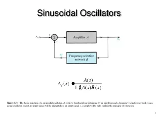
Oscillator Model • Two-Port Network Oscillator Model : Kwangwoon University
Theory of Oscillator • Oscillation Condition of the Two-port network Oscillator: • 1. K < 1 • 2. • 3. 여기서 k는 active device의 stability factor이며, where, : 공진회로의 반사계수 : 능동소자의 입력 반사계수 : 능동소자의 출력 반사계수 : 부하정합회로의 부하 반사계수 Kwangwoon University
Negative Resistance • Positive Resistance와 Negative Resistance 개념: (a) (b) Kwangwoon University
발진기에 의해서 생긴 sine wave 는, 부성 저항의 크기가 부하저항 (Rload) • 의 크기와 같아질 정도로 감소할 때까지 증가(진행)한다. • 부성 저항의 크기가 부하저항과 같아질 때, sine wave의 크기는 고정되고, • 발진기는 정상상태가 된다. • 정상 상태는 부성 저항에서 발생된 ac power가 부하 저항에서 발생된 생성 • 된 ac power와 정확히 같게 됨을 의미한다. • 이러한 간단한 부성저항 모델로부터 발진동작을 위한 중요한 2가지 규칙 • 을 유추해 낼 수 있다 Kwangwoon University
Oscillation Condition 1. 초기 발진 조건 발진이 시작하기 위해서, 부성저항의 크기가 부하저항보다 커야 한다 2. 정상 상태 발진 조건 부성저항의 크기가 부하 저항과 같아지면 발진변동이 멈춘다 where, Pss=정상상태 출력 전력 Kwangwoon University
Transistor Oscillator Kwangwoon University
Operating Theory • DC Power : Bias Voltage의 형태로 인가 • Feedback Loop : Transistor의 Impedance를 부성저항으로 변화시킴 • 발진조건이 충족되면, 공진기의 공진 주파수에서 발진이 발생 • 하고, AC전력이 부하에 전달 • 변환효율(Conversion Efficiency)은 부하에 전달된 AC 와 DC전력의 비 • Transistor의 부성 저항의 크기가 공진기의 양성저항보다 크고, • 공진기와 Tr.의 Reactance 성분이 반대 극성을 갖고 크기가 같을 때 • 발진이 시작됨 Kwangwoon University
Oscillation Condition 1. 초기 발진 조건 2. 정상상태 발진 조건 여기서 ZR: :Impedance of the Resonator ZT : Impedance of the Transistor Kwangwoon University
FET Oscillator • 유전체 기판에 FET를 장착시켜 임의의 특성 임피던스를 갖는 • 마이크로스트립 라인을 연결한 기본적인 초고주파 발진기 • 마이크로 스트립 공진기를 사용하기 때문에 회로구성이 간단하고, 게 • 이트, 소스, 드레인등의 3단자를 가지고 있기 때문에 다양한 능동 발진 • 회로를 구현할 수 있으며, 이런 특성을 이용하여, 변조, 보상을 제공함 • 으로써 발진기 동작의 제어를 가능하게 한다. • 주파수 Trimming 이 양호하지 못하며, 온도에 대한 안정도가 여타 다 • 른 발진기에 비해 떨어진다 Kwangwoon University
Type of FET Oscillator • 공통 게이트(C.G.) 구성 • - 저출력 발진기에 적합 • - 쉽게 발진하며 주파수 튜닝이 간편 • 공통 소오스(C.S.) 구성 • - 효율이 높다 • - 튜닝범위는 작으나 쉽게 튜닝이 가능 • - 높은 출력을 얻을 수 있다 • 공통 드레인(C.D.) 구성 • - 궤환 없이도 쉽게 발진 • - 높은 출력을 얻을 수 있다 • - 이득이 낮다 Kwangwoon University
Dielectric Resonator Oscillator • Stabilized DRO • Stable DRO • Series Feedback Oscillator Kwangwoon University
Stabilized DRO • Stabilized DRO는 반사형에 속하며, 발진주파수를 안정시키기 위해서 유전 • 체 공진기를 출력단에 위치시킨 것으로, 이때 유전체 공진기는 대역통과 필 • 터로서 작용하게 된다. • 그러나, 이 형태는 다음과 같은 단점을 가지고 있다. • - Phase Noise가 나쁘다 - 튜닝범위가 좁다 - 기생발진이 생긴다 (a) Stabilized DRO Kwangwoon University
Stable DRO • Stable DRO는 궤환형 (feedback)으로 분류되며 여기에는 병렬 궤환 (shunt • feedback)과 직렬 궤환 (series feedback)으로 나눌 수 있다. • 병렬 궤환 발진기는 FET gate 와 source 또는 gate 와 drain 회로사이에 유전 • 체 공진기를 궤환 요소로써 직접 이용한다. • 이 형태는 다음과 같은 특징을 가지고 있다 • - 해석이 복잡하다 - 튜닝범위가 좁다 - 상대적으로 출력이 낮다 (b) Stable DRO (병렬궤환) Kwangwoon University
Series Feedback Oscillator • 직렬 궤환 발진기는FET의 입력단에 유전체 공진기를 위치시킨 것으로 • 공진주파수 근처에서 마이크로스트립 전송로와 유전체 공진기는 강하게 • 결합되어, 이때 전력이 FET측으로 반사되어 FET는 불안정해지고 발진 • 이 일어나게 된다. 이 형태는 다음과 같은 장점을 가지고 있다. • - 기생발진을 피할 수 있다 • - 부하 변화에 대한 발진 주파수 및 출력 전력 변화가 적다 (c) Stable DRO (직렬궤환) Kwangwoon University
Single Oscillator Design • 직렬 궤환 구조를 갖는 Hairpin 공진기 발진기 Kwangwoon University
발진기의 선형 설계 • 위상 조건과 부성저항 발생조건을 만족시키기 위해 • l1 , l2의 길이를 조절. • 부성 저항 특성을 좋게 하기 위해 Open Stub를 이용함 • l1 : • - Transistor의 gate port로부터의 길이 • - Hairpin 공진기와 microstrip 선로와의 결합이 최대가 되도록 조절 • l2 : • - Transistor의 gate 단에서 바라본 반사 계수가 최대가 되도록 • l2의 길이를 조정하여 최적화 Kwangwoon University
Design Tip : • 발진 주파수를 쉽게 조정하기 위해서, • - Hairpin 공진기의 병렬 결합 선로를 조절 • - 부성저항의 대역폭을 가능한한 넓게 함 • 출력을 최적화 하기 위해서, • - 출력 단자의 정합 Stub인 l3를 조절함 Kwangwoon University
DC Bias 회로 • 설계 원칙 : • DC Bias는 발진기의 RF 동작에 최소한의 영향을 주면서 소자에 공급 • DC Bias는 발진기에 의해서 발생된 RF energy로부터 잘 분리되어 공급 • Capacitor 와 inductor는 Bias 회로의 중요한 구성 요소 : • Capacitor 는 DC Open 회로와 RF Short 회로로써 사용, • Inductor 는 DC Short 회로와 RF Open 회로로써 동작. Kwangwoon University
고주파에서는 Lumped Inductance를 구현하기 힘듦 • (b) 에서 보는 바와 같이 Microstrip으로 대신 가능 (a) (b) Kwangwoon University
RF Short Circuit은 그림 (c)에서 보는 바와 같이 Microstrip Radial Stub로 • 부터 얻을 수 있다. (c) Kwangwoon University
Bias 회로의 Layout과 특성 곡선 • (유전율: 10, 중심주파수 : 9 GHz) Kwangwoon University
Layout of the single Oscillator • HP EEsof Libra ver. 6.1 Kwangwoon University
Schematic of the single Oscillator Kwangwoon University
Oscillation Possibility of the Single Oscillator Kwangwoon University
Output Power & Voltage Waveform of the Single Oscillator Kwangwoon University
Dielectric Resonator Oscillator Using Series Feedback Kwangwoon University
DR Resonator 와 Microstrip line 의 관계 • DR is mounted close to a microstrip line • D : determines the coupling between the resonator and microstrip line Kwangwoon University
DR 공진 발진기의 Schematic 구조 Kwangwoon University
Dielectric Resonator Design DR 공진기 회로 모델 ( 5.8 GHz ) R = 2000 L = 9.15e-03 nH C = 82.34 pF Kwangwoon University
Simulation Result of Dielectric Resonator = -0.43dB @ 5.8 GHz = -24.3 dB @ 5.8 GHz Kwangwoon University
DR Oscillator Schematic Design Kwangwoon University
DR Oscillator Layout Design • HP EEsof Libra ver. 6.1 Kwangwoon University