Shift Register
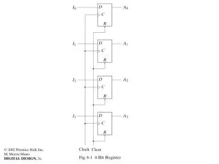
Shift Register. Section 6.1-6.2. Register. A register is a group of flip-flops, each one of which is capable of storing one bit of information. Issues of the circuit to the right. You do not have an option hold the output when you don’t want to outputs updated.

Shift Register
E N D
Presentation Transcript
Shift Register Section 6.1-6.2
Register • A register is a group of flip-flops, each one of which is capable of storing one bit of information. • Issues of the circuit to the right. • You do not have an option hold the output when you don’t want to outputs updated. 4 D flip-flops=4 bits of storage=4-bit register
Load=“1”→Update I0 is fed to DFF when Load is a 1. “0” “1” “1” “0” “I0” “I0”
Load=“0”→Hold! A0 is fed to DFF when Load is a 0. So the output is holding! “1” “0” “0” “A0” “A0” “0” We will revisit this idea when we study the universal shift register.
Four-Bit Serial Shift Register 1 2 3 4 Q of DFF1 gets SI after the first rising edge of the CLK Q of DFF2 gets SI after the second rising edge of the CLK Q of DFF3 gets SI after the third rising edge of the CLK Q of DFF4 gets SI after the fourth rising edge of the CLK
Linear Feedback Shift Register Exclusive OR
Block Diagram of a Universal Shift Register This is called the universal shift register because it has both shifts and parallel load capabilities.
Functionality of the Universal Shift Register Clear: to clear the register to 0. CLK: to synchronize the operations. {S1,S0} for mode control. A_par: register output I_par: register input MSB_inand LSB_in: serial inputs
Four-to-one-line Mux 0 0 0 0 I2 I2 I2 1 0 1 0 1 0
S0=0, S1=0 [No Change Mode] S0=0, S1=0
S0=1, S1=0 [Shift Right Mode] S1=0 , S0=1
S0=0, S1=1 [Shift Left Mode] S1=1 , S0=0
S0=1, S1=1 [Parallel Load Mode] S1=1 , S0=1
Breadboard Implementation Universal shift regsiter Random Number Generator
Waveform Random A3 A2 A1 A0 CLK
Behavioral Vs. Structural Description • Behavioral Description • Behavior model of a shift register • Describe the operation of the register without a preconceived structure. • Random number generator • Binary values of msb_in, lsb_in, i_par • Structural Description • Models the circuits in terms of a collection of components such as gates, flip-flops…
Test Bench Test all input combinations by flipping {S1, S0} 1. Generate random number With matlab Read random number at the neg edge of the clock Read numbers to i_par[3:0],msb_in, lsb_in at the negedge of t_clock
[s1,s0=[1,1], Load i_par=0111 a_par=0111
[s1,s0]=[0,0], No Change i_par=0111 a_par=0011
[s1,s0]=[1,0], Shift Left 1101 1011 LSB_in
Structural Modeling of a 4-Bit Universal Shift Register Q clr clk select i3 i1 i0 i2
Waveform Load No Change Shift Right Shift Left
Load=“1”→Update I0 is fed to DFF when Load is a 1. “0” “1” “1” “0” “I0” “I0”
Load=“0”→Hold! A0 is fed to DFF when Load is a 0. So the output is holding! “1” “0” “0” “A0” “A0” “0” We will revisit this idea when we study the universal shift register.
S0=0, S1=0 [No Change Mode] S0=0, S1=0
S0=1, S1=0 [Shift Right Mode] S1=0 , S0=1
S0=0, S1=1 [Shift Left Mode] S1=1 , S0=0
S0=1, S1=1 [Parallel Load Mode] S1=1 , S0=1
Serial Transfer Using Shift Register Information in A is made to circulate by connecting SO to SI.
Parallel Transfer Versus Serial Transfer (Serial Transfer) Take multiple clock cycles to transfer data. Assume n=4, each shift Register has 4 DFF. Parallel Transfer Transfer all the bit in one clock cycle. Require combinatorial circuits.
Augend, Addend & Sum 1011 +1001 ______ 10100 Augend Addend Sum
Serial Adder Assuming a shift-right register, the left most position becomes available for storage after the second rising edge of the clock. 1 0 (Augend) 1 1 Feed “1” to z at the next rising edge of the CLK (Addend) Note that The sum can be stored in a third register. But if you want to save shift register, you can store it in A since more and more slots in SRA become available.
Serial Adder At the end of T4 S3 S2S1S0A3 Co D2D1D0B3 A3A2A1A0 B3B2B1B0 ________________ CoS3S2S1S0
Allowing the Serial Adder to Accumulate T3 T2T1T0S3 Ro X2X1X0D3 Co S3 S2 S1S0 D3D2D1D0 ________________ Ro T3 T2 T1 T0
Accumulate with a Shift Register • A, B and D, each represents a 4 bit sequence. • We want to perform A+B+D • Store A in shift register A. • Store B in shift register B. • Allow the CLK to go on for a couple of cycles. • Store the sum bits of A+B in Shift A and allow D to enter shift register B. • Allow more cycles of CLK. • Add D to A+B, and allow A+B+C to enter shift register A.

