Memory
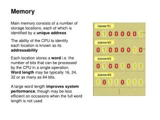
Memory. See: P&H Appendix C.8, C.9. Big Picture: Building a Processor. memory. register file. inst. alu. +4. +4. addr. =?. PC. d in. d out. control. cmp. offset. memory. new pc. target. imm. extend. A Single cycle processor. Goals for today. Review Finite State Machines

Memory
E N D
Presentation Transcript
Memory See: P&H Appendix C.8, C.9
Big Picture: Building a Processor memory registerfile inst alu +4 +4 addr =? PC din dout control cmp offset memory new pc target imm extend A Single cycle processor
Goals for today Review • Finite State Machines Memory • Register Files • Tri-state devices • SRAM (Static RAM—random access memory) • DRAM (Dynamic RAM)
Example: Digital Door Lock • Digital Door Lock • Inputs: • keycodes from keypad • clock • Outputs: • “unlock” signal • display how many keys pressed so far
Door Lock: Inputs • Assumptions: • signals are synchronized to clock • Password is B-A-B K A B
Door Lock: Outputs • Assumptions: • High pulse on U unlocks door LEDdec 4 8 D3D2D1D0 U
Door Lock: Simplified State Diagram Ø Ø “A” “B” G3 G1 G2 ”3”, U ”1” ”2” else else “B” any Idle ”0” Ø else any else else B1 B2 B3 ”1” ”2” ”3” Ø Ø
Door Lock: Simplified State Diagram Ø Ø “A” “B” G3 G1 G2 ”3”, U ”1” ”2” else else “B” any Idle ”0” else Ø else else B1 B2 ”1” ”2” Ø Ø
Door Lock: Simplified State Diagram Ø Ø “A” “B” G3 G1 G2 ”3”, U ”1” ”2” else else “B” any Idle ”0” else Ø else else B1 B2 ”1” ”2” Ø Ø
Door Lock: Simplified State Diagram Ø Ø “A” “B” G3 G1 G2 ”3”, U ”1” ”2” else else “B” any Idle ”0” else Ø else else B1 B2 ”1” ”2” Ø Ø
State Table Encoding R P 4 8 D3D2D1D0 Q dec U
Door Lock: Implementation 4 D3-0 dec S2-0 3bitReg U clk S2-0 A S’2-0 B C Strategy: (1) Draw a state diagram (e.g. Moore Machine) (2) Write output and next-state tables (3) Encode states, inputs, and outputs as bits (4) Determine logic equations for next state and outputs
Administrivia • Make sure partner in same Lab Section this week Lab2 is out • Due in one week, next Monday, start early • Work alone • But, use your resources • Lab Section, Piazza.com, Office Hours, Homework Help Session, • Class notes, book, Sections, CSUGLab No Homework this week
Administrivia Check online syllabus/schedule • http://www.cs.cornell.edu/Courses/CS3410/2012sp/schedule.html • Slides and Reading for lectures • Office Hours • Homework and Programming Assignments • Prelims (in evenings): • Tuesday, February 28th • Thursday, March 29th • Thursday, April 26th Schedule is subject to change
Collaboration, Late, Re-grading Policies • “Black Board” Collaboration Policy • Can discuss approach together on a “black board” • Leave and write up solution independently • Do not copy solutions Late Policy • Each person has a total of four “slip days” • Max of two slip days for any individual assignment • Slip days deducted first for any late assignment, cannot selectively apply slip days • For projects, slip days are deducted from all partners • 20% deducted per day late after slip days are exhausted Regrade policy • Submit written request to lead TA, and lead TA will pick a different grader • Submit another written request, lead TA will regrade directly • Submit yet another written request for professor to regrade.
Goals for today Review • Finite State Machines Memory • Register Files • Tri-state devices • SRAM (Static RAM—random access memory) • DRAM (Dynamic RAM)
Register File • Register File • N read/write registers • Indexed by register number • Implementation: • D flip flops to store bits • Decoder for each write port • Mux for each read port Dual-Read-PortSingle-Write-Port 32 x 32 Register File QA 32 DW 32 QB 32 W RW RA RB 1 5 5 5
Register File • Register File • N read/write registers • Indexed by register number • Implementation: • D flip flops to store bits • Decoder for each write port • Mux for each read port Dual-Read-PortSingle-Write-Port 32 x 32 Register File QA 32 DW 32 QB 32 W RW RA RB 1 5 5 5
Register File • Register File • N read/write registers • Indexed by register number • Implementation: • D flip flops to store bits • Decoder for each write port • Mux for each read port Dual-Read-PortSingle-Write-Port 32 x 32 Register File QA 32 DW 32 QB 32 W RW RA RB 1 5 5 5
Tradeoffs • Register File tradeoffs + Very fast (a few gate delays for both read and write) + Adding extra ports is straightforward – Doesn’t scale
Building Large Memories • Need a shared bus (or shared bit line) • Many FFs/outputs/etc. connected to single wire • Only one output drives the bus at a time
Tri-State Devices Tri-State Buffers E E Vdd D Q D D Q Gnd
Tri-State Devices Tri-State Buffers E E Vdd D Q D D Q Gnd
Shared Bus D0 S0 D1 S1 D2 S2 D3 S3 D1023 S1023 shared line
SRAM • Static RAM (SRAM) • Essentially just SR Latches + tri-states buffers
SRAM Chip row decoder A21-10 CSR/W column selector, sense amp, and I/O circuits A9-0 Shared Data Bus
SRAM Cell • Typical SRAM Cell bit line word line B B • Each cell stores one bit, and requires 4 – 8 transistors (6 is typical) • Read: • pre-charge B and B to Vdd/2 • pull word line high • cell pulls B or B low, sense amp detects voltage difference • Write: • pull word line high • drive B and B to flip cell
SRAM Modules and Arrays R/W 1M x 4SRAM 1M x 4SRAM 1M x 4SRAM 1M x 4SRAM A21-0 CS msb lsb CS Bank 2 CS Bank 3 CS Bank 4
SRAM Summary • SRAM • A few transistors (~6) per cell • Used for working memory(caches) • But for even higher density…
Dynamic RAM: DRAM bit line • Dynamic-RAM (DRAM) • Data values require constant refresh word line Capacitor Gnd
DRAM vs. SRAM • Single transistor vs. many gates • Denser, cheaper ($30/1GB vs. $30/2MB) • But more complicated, and has analog sensing • Also needs refresh • Read and write back… • …every few milliseconds • Organized in 2D grid, so can do rows at a time • Chip can do refresh internally • Hence… slower and energy inefficient
Memory • Register File tradeoffs + Very fast (a few gate delays for both read and write) + Adding extra ports is straightforward – Expensive, doesn’t scale – Volatile • Volatile Memory alternatives: SRAM, DRAM, … – Slower + Cheaper, and scales well – Volatile Non-Volatile Memory (NV-RAM): Flash, EEPROM, … + Scales well – Limited lifetime; degrades after 100000 to 1M writes
Summary • We now have enough building blocks to build machines that can perform non-trivial computational tasks • Register File: Tens of words of working memory • SRAM: Millions of words of working memory • DRAM: Billions of words of working memory • NVRAM: long term storage (usb fob, solid state disks, BIOS, …) • Next time we will build a simple processor!

