Memory
Memory. Secondary Memory Primary Memory RAM SRAM DRAM ROM PROM EPROM Hybrid EEPROM NVRAM Flash Memory Cache Memory Virtual Memory. Memory Types.

Memory
E N D
Presentation Transcript
Secondary Memory • Primary Memory • RAM • SRAM • DRAM • ROM • PROM • EPROM • Hybrid • EEPROM • NVRAM • Flash Memory • Cache Memory • Virtual Memory Memory Types
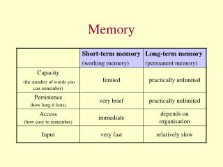
The computer usually uses its input/output channels to access secondary storage and transfers the desired data using intermediate area in primary storage. Secondary storage does not lose the data when the device is powered down—it is non-volatile. Per unit, it is typically also an order of magnitude less expensive than primary storage. • The secondary storage is often formatted according to a file system format, which provides the abstraction necessary to organize data into files and directories, providing also additional information (called metadata) describing the owner of a certain file, the access time, the access permissions, and other information. Hard disk are usually used as secondary storage. Secondary Memory
Primary storage (or main memory or internal memory), often referred to simply as memory, is the only one directly accessible to the CPU. The CPU continuously reads instructions stored there and executes them as required. • Main memory is directly or indirectly connected to the CPU via a memory bus. It is actually two buses (not on the diagram): an address bus and a data bus. The CPU firstly sends a number through an address bus, a number called memory address, that indicates the desired location of data. Then it reads or writes the data itself using the data bus. • It is divided into RAM and ROM. Primary Memory
The RAM family includes two important memory devices: static RAM (SRAM) and dynamic RAM (DRAM). The primary difference between them is the lifetime of the data they store. SRAM retains its contents as long as electrical power is applied to the chip. If the power is turned off or lost temporarily, its contents will be lost forever. DRAM, on the other hand, has an extremely short data lifetime-typically about four milliseconds. This is true even when power is applied constantly. DRAM controller is used to refresh the data before it expires, the contents of memory can be kept alive for as long as they are needed. So DRAM is as useful as SRAM after all. RAM
Double Data Rate synchronous dynamic random access memory or also known as DDR1 SDRAM is a class of memory integrated circuits used in computers. The interface uses double pumping (transferring data on both the rising and falling edges of the clock signal) to lower the clock frequency. One advantage of keeping the clock frequency down is that it reduces the signal integrity requirements on the circuit board connecting the memory to the controller. Types of RAM
DDR2 memory is fundamentally similar to DDR SDRAM. Still, while DDR SDRAM can transfer data across the bus two times per clock, DDR2 SDRAM can perform four transfers per clock. DDR2 uses the same memory cells, but doubles the bandwidth by using the multiplexing technique. The DDR2 memory cell is still clocked at the same frequency as DDR SDRAM and SDRAM cells, but the frequency of the input/output buffers is higher with DDR2 SDRAM (as shown in Fig. on next Slide). The bus that connects the memory cells with the buffers is twice wider compared to DDR. Thus, the I/O buffers perform multiplexing: the data is coming in from the memory cells along a wide bus and is going out of the buffers on a bus of the same width as in DDR SDRAM, but of a twice bigger frequency. This allows to increase the memory bandwidth without increasing the operational frequency. DDR2, DDR and SDRAM
The interface uses double pumping (transferring data on both the rising and falling edges of the clock signal to lower the clock frequency. One advantage of keeping the clock frequency down is that it reduces the signal integrity requirements on the circuit board connecting the memory to the controller.
Memories in the ROM family are distinguished by the methods used to write new data to them (usually called programming), and the number of times they can be rewritten. This classification reflects the evolution of ROM devices from hardwired to programmable to erasable-and-programmable. A common feature is their ability to retain data and programs forever, even during a power failure. The contents of the ROM had to be specified before chip production, so the actual data could be used to arrange the transistors inside the chip. Types of ROM
One step up from the masked ROM is the PROM (programmable ROM), which is purchased in an unprogrammed state. If you were to look at the contents of an unprogrammed PROM, the data is made up entirely of 1's. The process of writing your data to the PROM involves a special piece of equipment called a device programmer. The device programmer writes data to the device one word at a time by applying an electrical charge to the input pins of the chip. Once a PROM has been programmed in this way, its contents can never be changed. If the code or data stored in the PROM must be changed, the current device must be discarded. As a result, PROMs are also known as one-time programmable (OTP) devices. PROM
An EPROM (erasable-and-programmable ROM) is programmed in exactly the same manner as a PROM. However, EPROMs can be erased and reprogrammed repeatedly. To erase an EPROM, you simply expose the device to a strong source of ultraviolet light. (A window in the top of the device allows the light to reach the silicon.) By doing this, you essentially reset the entire chip to its initial-unprogrammed-state. Though more expensive than PROMs, their ability to be reprogrammed makes EPROMs an essential part of the software development and testing process. EPROM
As memory technology has matured in recent years, the line between RAM and ROM has blurred. Now, several types of memory combine features of both. These devices do not belong to either group and can be collectively referred to as hybrid memory devices. Hybrid memories can be read and written as desired, like RAM, but maintain their contents without electrical power, just like ROM. Two of the hybrid devices, EEPROM and flash, are descendants of ROM devices. These are typically used to store code. The third hybrid, NVRAM, is a modified version of SRAM. NVRAM usually holds persistent data. Hybrid types
EEPROMS are electrically-erasable-and-programmable. Internally, they are similar to EPROMs, but the erase operation is accomplished electrically, rather than by exposure to ultraviolet light. Any byte within an EEPROM may be erased and rewritten. Once written, the new data will remain in the device forever-or at least until it is electrically erased. The primary tradeoff for this improved functionality is higher cost, though write cycles are also significantly longer than writes to a RAM. So you wouldn't want to use an EEPROM for your main system memory.
Flash memory combines the best features of the memory devices described thus far. Flash memory devices are high density, low cost, nonvolatile, fast (to read, but not to write), and electrically reprogrammable. These advantages are overwhelming and, as a direct result, the use of flash memory has increased dramatically in embedded systems. From a software viewpoint, flash and EEPROM technologies are very similar. The major difference is that flash devices can only be erased one sector at a time, not byte-by-byte. Typical sector sizes are in the range 256 bytes to 16KB. Despite this disadvantage, flash is much more popular than EEPROM and is rapidly displacing many of the ROM devices as well.
The third member of the hybrid memory class is NVRAM (non-volatile RAM). Nonvolatility is also a characteristic of the ROM and hybrid memories discussed previously. However, an NVRAM is physically very different from those devices. An NVRAM is usually just an SRAM with a battery backup. When the power is turned on, the NVRAM operates just like any other SRAM. When the power is turned off, the NVRAM draws just enough power from the battery to retain its data. NVRAM is fairly common in embedded systems. However, it is expensive-even more expensive than SRAM, because of the battery-so its applications are typically limited to the storage of a few hundred bytes of system-critical information that can't be stored in any better way.
A CPU cache is a cache used by the centralprocessing unit of a computer to reduce the average time to access memory. The cache is a smaller, faster memory which stores copies of the data from the most frequently used main memory locations. As long as most memory accesses are cached memory locations, the average latency of memory accesses will be closer to the cache latency than to the latency of main memory. • When the processor needs to read from or write to a location in main memory, it first checks whether a copy of that data is in the cache. If so, the processor immediately reads from or writes to the cache, which is much faster than reading from or writing to main memory Cache Memory
The diagram on the right shows two memories. Each location in each memory has a datum (a cache line), which in different designs ranges in size from 8 to 512 bytes. The size of the cache line is usually larger than the size of the usual access requested by a CPU instruction, which ranges from 1 to 16 bytes. Each location in each memory also has an index, which is a unique number used to refer to that location.The index for a location in main memory is called an address. Each location in the cache has a tag that contains the index of the datum in main memory that has been cached. In a CPU's data cache these entries are called cache lines or cache blocks. Cache Memory
Virtual Memory It is a computer system technique which gives an application program the impression that it has contiguous working memory (an address space), while in fact it may be physically fragmented and may even overflow on to disk storage. computer operating systems generally use virtual memory techniques for ordinary applications, such as word processors, spreadsheets,multimedia,players accounting, etc., except where the required hardware support (memory management unit) is unavailable or insufficient.


