
Uploaded by
chick
1 SLIDES
129 VUES
10LIKES
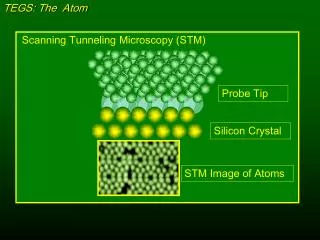
High-Resolution STM Imaging of Silicon Crystal Atoms Using Scanning Tunneling Microscopy
DESCRIPTION
This study explores the use of Scanning Tunneling Microscopy (STM) to obtain high-resolution images of silicon crystal atoms. By employing a finely tuned STM probe tip, researchers achieved remarkable visualization of atomic structures on silicon substrates. The detailed images provide insights into atomic arrangements and electronic properties, impacting fields such as nanotechnology and material science. This advancement in STM not only enhances our understanding of silicon but also opens pathways for future research in nano-scale engineering and semiconductor development.
Download
1 / 1
Télécharger la présentation 
High-Resolution STM Imaging of Silicon Crystal Atoms Using Scanning Tunneling Microscopy
An Image/Link below is provided (as is) to download presentation
Download Policy: Content on the Website is provided to you AS IS for your information and personal use and may not be sold / licensed / shared on other websites without getting consent from its author.
Content is provided to you AS IS for your information and personal use only.
Download presentation by click this link.
While downloading, if for some reason you are not able to download a presentation, the publisher may have deleted the file from their server.
During download, if you can't get a presentation, the file might be deleted by the publisher.
E N D
Presentation Transcript
TEGS: The Atom Scanning Tunneling Microscopy (STM) Probe Tip Silicon Crystal STM Image of Atoms


More Related