Download
1 / 43
640 likes | 1.42k Vues
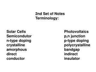
Solar Cell Chapter 3. Semiconductors and P-N Junction. Nji Raden Poespawati Department of Electrical Engineering Faculty of Engineering University of Indonesia . Contents. 3.1. Basic 3.2. Generation 3.3. Recombination 3.4. Carrier Transport 3.5. P-N Junctions. Basic.

E N D
Solar CellChapter 3. Semiconductors and P-N Junction Nji Raden Poespawati Department of Electrical Engineering Faculty of Engineering University of Indonesia
Contents 3.1.Basic 3.2. Generation 3.3. Recombination 3.4. Carrier Transport 3.5. P-N Junctions
Basic • Semiconductor Structure • The structure of a semiconductor is shown in Figure 1. • Section from the periodic table (see Figure 2) and Figure 3 depicts an animation showing formation of "free" electrons and holes when an electron can escape its bond. • The most important parameters of a semiconductor material for solar cell operation are: • the band gap; • the number of free carriers available for conduction; and • the "generation" and recombination of free carriers in response to light shining on the material.
Basic(continued) • Band Gap • The band gap of a semiconductor is the minimum energy required to move an electron from its bound state to a free state where it can participate in conduction.(See Figure 4) • Intrinsic Carrier Concentration • The concentration of these carriers is called the intrinsic carrier concentration, denoted by ni. • Figure 5 shows Intrinsic carrier concentration in a semiconductor at two temperatures.
Basic(continued) • Doping • It is possible to shift the balance of electrons and holes in a silicon crystal lattice by "doping" it with other atoms.(see Figure 6) • In doped material: • the type of carrier with the higher concentration is called a "majority carrier", • while the lower concentration carrier is called a "minority carrier." • The table 1 summarizes the properties of semiconductor types. • Equilibrium Carrier Concentration • The number of carriers in the conduction and valence band with no externally applied bias is called the equilibrium carrier concentration.
Basic(continued) • At equilibrium, the product of the majority and minority carrier concentration is a constant, and this is mathematically expressed by the Law of Mass Action. n0p0 = ni2 ………………..(3.1) • where ni is the intrinsic carrier concentration and n0 and p0 are the electron and hole equilibrium carrier concentrations.
Basic(continued) • Using the Law of Mass Action above, the majority and minority carrier concentrations are given as: • Figure 7 illustrates minority carrier of n-type material
Generation • Absorption of Light • Photons incident on the surface of a semiconductor : • reflected from the top surface, • absorbed in the material or, • transmitted through the material. • A key factor in determining if a photon is absorbed or transmitted is the energy of the photon.
Generation(continued) • There are three groups based on their energy compared to that of the semiconductor band gap: • Eph < EG Photons with energy Eph less than the band gap energy EGinteract only weakly with the semiconductor, passing through it as if it were transparent. • Eph = EG have just enough energy to create an electron hole pair and are efficiently absorbed. • Eph > EG Photons with energy much greater than the band gap are strongly absorbed
Generation(continued) • Absorption Coefficient • The absorption coefficient determines how far into a material light of a particular wavelength can penetrate before it is absorbed. • The absorption coefficient depends on the material and also on the wavelength of light which is being absorbed. • The absorption coefficient for several semiconductor materials is shown in Figure 8.
Generation(continued) • Absorption Depth • The absorption depth is given by the inverse of the absorption coefficient, or a-1. • The variation in the absorption depth for "blue" and "red" photons is shown in Figure 9. • The absorption depths for several semiconductors are shown in Figure 10.
Generation(continued) • Generation Rate • The generation rate gives the number of electrons generated at each point in the device due to the absorption of photons. • The intensity of light at any point in the device can be calculated according to the equation: …………….(3.2) where a is the absorption coefficient typically in cm-1;x is the distance into the material at which the light intensity is being calculated; and I0 is the light intensity at the top surface.
Generation(continued) • differentiating the above equation will give the generation at any point in the device. Hence: ……….(3,3) • where N0 = photon flux at the surface (photons/unit-area/sec.); a = absorption coefficient; and x = distance into the material. • The generation rate at three different wavelengths for silicon is shown in Figure 11 • Figure 12 shows The generation as a function of distance for a standard solar spectrum incident on a piece of silicon.
Recombination • Types of Recombination • when the electron falls back down into the valence band, it also effectively removes a hole. This process is called recombination. • There are three basic types of recombination in the bulk of a single-crystal semiconductor. These are: • Radiative recombination; • Auger recombination; and • Shockley-Read-Hall recombination. • These are described in the animation and text in Figure 13.
Recombination(continued) Radiative Recombination • Radiative recombination is the recombination mechanism which dominates in devices such as LEDs and lasers. • The key characteristics of radiative recombination are: • In radiative recombination, an electron directly combines with a hole in the conduction band and releases a photon; and • The emitted photon has an energy similar to the band gap and is therefore only weakly absorbed such that it can exit the piece of semiconductor.
Recombination(continued) Recombination Through Defect Levels • Recombination through defects, also called Shockley-Read-Hall or SRH recombination, does not occur in perfectly pure, undefected material. • SRH recombination is a two-step process. The two steps involved in SRH recombination are: • An electron (or hole) is trapped by an energy state in the forbidden region which is introduced through defects in the crystal lattice. and • If a hole (or an electron) moves up to the same energy state before the electron is thermally re-emitted into the conduction band, then it recombines.
Recombination(continued) Auger Recombination • An Auger Recombination involves three carriers • An electron • a hole • heat or as a photon, • Auger recombination is most important in heavily doped or heavily excited material.
Recombination(continued) • Diffusion Length • the "minority carrier diffusion length" is the average distance a carrier can move from point of generation until it recombines • The minority carrier lifetime and the diffusion length depend strongly on the type and magnitude of recombination processes in the semiconductor
Recombination(continued) • Surface Recombination • Any defects or impurities within or at the surface of the semiconductor promote recombination • The dangling bonds at the surface of semiconductor cause a high local recombination rate
Carrier Transport • Movement of Carriers in Semiconductors • The velocity of the carriers is determined by the temperature of the lattice. • Carriers in a semiconductor crystal at a temperature T move on average with a velocity of 1/2mv2 where m is the mass of the carrier and v is the thermal velocity. • The thermal velocity is the average carrier velocity
Carrier Transport(continued) • Diffusion • Carriers flow from the high-concentration region to the low-concentration region. This carrier flow, called "diffusion", is caused by the random motion of carriers. (see Figure 14) • Drift • Transport due to the movement of carriers in an electric field is called "drift transport".
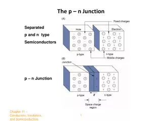
P-N Junctions • P-n Junction Diodes • P-n junction diodes form the basis not only of solar cells, but of many other electronic devices such as LEDs, lasers, photodiodes and bipolar junction transistors (BJTs). • Formation of a P-n junction • P-n junctions are formed by joining n-type and p-type semiconductor materials, • Figure 15 shows the animation of the formation of the Êat the junction between n and p-type material • Carrier Movement in Equilibrium
P-N Junctions(continued) • Bias of P-n Junctions • Semiconductor devices have three modes of operation: 1.Thermal Equilibrium 2. Steady State 3. Transient • Diodes under Forward Bias • Carrier Injection and Forward Bias Current Flow • Reverse Bias • In reverse bias
P-N Junctions(continued) • Diode Equation • Ideal Diodes • The Ideal Diode Law, expressed as: …………..(3.4) where:I = the net current flowing through the diode; I0 = "dark saturation current", the diode leakage current density in the absence of light; V = applied voltage across the terminals of the diode; q = absolute value of electron charge; k= Boltzmann's constant; and T = absolute temperature (K).
P-N Junctions(continued) • Non-Ideal Diodes • For actual diodes, the expression becomes: ………….(3.5) • where:n = ideality factor • The diode law which is illustrated for silicon, is in Figure 16.
Figure 1. Schematic representation of covalent bonds in a silicon crystal lattice
Figure 2. Section from the periodic table. More common semiconductor materials are shown in blue. A semiconductor can be either of a single element, such as Si or Ge, a compound, such as GaAs, InP or CdTe, or an alloy, such as SixGe(1-x) or AlxGa(1-x)As, where x is the fraction of the particular element and ranges from 0 to 1.
Figure 3. Animation showing formation of "free" electrons and holes when an electron can escape its bond.
Figure 4. Schematic of the energy bands for electrons in a solid.
Figure 5. Intrinsic carrier concentration in a semiconductor at two temperatures. Note that in both cases, the number of electrons and the number of holes is equal.
Figure 6.Schematic of a silicon crystal lattice doped with impurities to produce n-type and p-type semiconductor material.
P-type (positive) N-type (negative) Dopant Group III (E.g. Boron) Group V (e.g. Phosphorous) Bonds Missing Electrons (Holes) Excess Electrons Majority Carriers Holes Electrons Minority Carriers Electrons Holes Table 1. the properties of semiconductor types
Figure 7. Equilibrium carrier concentration for low and high doping, showing that as the doping increases, the minority carrier concentration decreases.
Figure 8. The absorption coefficient, a, in a variety of semiconductor materials at 300K as a function of the vacuum wavelength of light.
Figure 9. The blue photons are absorbed very close to the surface but most of the red photons are absorbed deep in the device.
Figure 10. The absorption depths for several semiconductors .
Figure 11. The generation rate in silicon for several wavelengths of light.
Figure 12. Generation rate of electron-hole pairs in a piece of silicon as a function of distance into the cell. The cell front surface is at 0 mm and is where most of the high energy blue light is absorbed.
Figure 15 shows the animation of the formation of the Êat the junction between n and p-type material
Figure 16. The diode law for silicon - current changes with voltage and temperature. For a given current, the curve shifts by approximately 2 mV/°C