Download
1 / 9
430 likes | 1.42k Vues
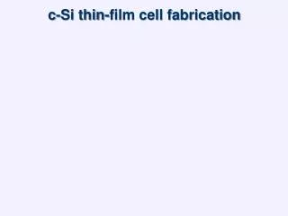
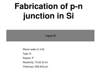
Fabrication of p-n junction in Si. n-type Si. Silicon wafer [1-0-0] Type : N Dopant : P Resistivity: 10-20 Ω-cm Thickness : 505-545 µm. SiO 2. Oxidize the Si wafer. n-type Si. Mask A . SiO 2. Load Mask A. Photo resist. n-type Si. Mask A. Remove exposed PR. Remove SiO 2.

E N D
Fabrication of p-n junction in Si n-type Si Silicon wafer [1-0-0] Type: N Dopant: P Resistivity: 10-20 Ω-cm Thickness: 505-545 µm
SiO2 Oxidize the Si wafer n-type Si
Mask A SiO2 • Load Mask A Photo resist n-type Si
Mask A Removeexposed PR RemoveSiO2 Photo resist SiO2 n-type Si
Implanted p region Implanted p region Removeunexposed PR Doping by ion implantation Windows SiO2 :::::::::: :::::::::: n-type Si B B
Al deposition for contacts Al Al SiO2 :::::::::: :::::::::: p region p region n-type Si
Lithography (Mask B) Mask B Photo resist Photo resist Al Al SiO2 :::::::::: :::::::::: p region p region n-type Si
Developer/Al Etching Mask B Photo resist :::::::::: :::::::::: SiO2 n-type Si
Removeunexposed PR p-n junction Photo resist Photo resist SiO2 :::::::::: :::::::::: p region p region n-type Si