Cluster Processor Chip
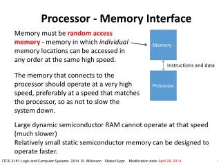
Cluster Processor Chip. Blocks overview Clock distributions Front-end synchronization Resources Constraints. CPM Final Design Review, Birmingham, 22 nd March 2005. CP chip layout. Clocks generator Synchronisation of Onboard /Backplane data BCDemux/ Parity check Algorithm Hit output

Cluster Processor Chip
E N D
Presentation Transcript
Cluster Processor Chip • Blocks overview • Clock distributions • Front-end synchronization • Resources • Constraints CPM Final Design Review, Birmingham, 22nd March 2005
CP chip layout • Clocks generator • Synchronisation of Onboard/Backplane data • BCDemux/ Parity check • Algorithm • Hit output • Readout
CP Chip: Clock generator Deskew2_40 Deskew2_40 DLL Deskew2_160 Deskew2_40_delayed Deskew2_160_delayed DLL Deskew1_40 Deskew1_40
CP Chip: Front-end Synchronization: Backplane Data Select_Clk Data_Backplane F/F MUX Data_Backplane Deskew2_160 F/F Data_Backplane F/F Deskew2_160 Deskew2_160_delayed
CP Chip: Front-End Synchronization: On-Board Data Data_Onboard Data_Onboard F/F F/F Deskew2_160_delayed Deskew2_160
CP Chip: Data processing BCDemux Algorithm RoI Data Data_Backplane Srl to Parallel Data_Onboard Deskew2_160 Hit Deskew2_40
CP Chip: Readout RoI Deskew2_40 Wr Deskew1_40 Data_RoI Rd
CP Chip: Resources • Logic Utilization: • Number of Slice Flip Flops: 6,413 out of 24,576 26% Number of 4 input LUTs: 15,177 out of 24,576 61% • Logic Distribution: Number of occupied Slices: 10,041 out of 12,288 81% • Total Number 4 input LUTs: 15,502 out of 24,576 63% Number used as logic: 15,177 Number used as a route-thru: 323 Number used as Shift registers: 2 • Number of bonded IOBs: 184 out of 404 45% IOB Flip Flops: 18 Number of Tbufs: 208 out of 12,544 1% Number of Block RAMs: 6 out of 96 6% Number of GCLKs: 4 out of 4 100% Number of GCLKIOBs: 3 out of 4 75% Number of DLLs: 4 out of 8 50%
CP Chip: Constraints file • Main part of the constraint file is to place the F/F of the synchronization blocks as close as possible to the I/O pins : inst "I0_I2_I5_g1_5_I1_I0_reg_Q" LOC="CLB_R58C88.S0"; inst "I0_I2_I5_g1_5_I1_I1_reg_Q" LOC="CLB_R57C88.S0"; inst "I0_I2_I5_g1_5_I1_I2_reg_Q" LOC="CLB_R57C88.S1"; Done by physically allocating Xilinx CLB . • Other constraints deal with signal levels