
Matrix Keypad Analysis: No Key Press Scenario
E N D
Presentation Transcript
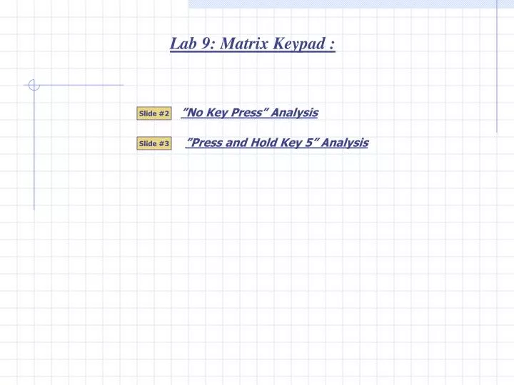
Lab 9: Matrix Keypad : ”No Key Press” Analysis Slide #2 ”Press and Hold Key 5” Analysis Slide #3
This symbol indicates counting…changing 1/0. The output of the counter is cycling (counting) very quickly because of the 1 K PPS clock signal. Each count state lasts only 1 millisecond. It only takes 16 milliseconds for the counter to complete cycle through its count states from 0 to 15. 1 0 1 0 0 1 1 0 1 0 0 0 1 1 1 0 0 0 1 1 1 0 1 0 0 0 1 0 1 0 1 1 1 0 1 0 0 0 1 1 0 1 1 0 1 0 0 1 0 1 0 1 0 1 0 1 0 1 1 1 0 1 0 0 Column #0 Column #1 Column #2 Column #3 0 1 0 1 0 0 1 0 0 1 1 0 1 0 1 1 1 1 1 0 1 1 1 0 0 1 1 1 1 1 1 0 1 1 0 1 0 1 1 1 1 1 1 0 1 1 0 1 1 Row #0 1 Row #1 1 1 Row #2 1 Row #3 1 0 The 0 cycling on the keypad columns and the MUX transferring the keypad row data is called scanning the keypad. This scanning will allow keys to be encoded. Lab 9 : “No key pressed” Analysis : A matrix keypad has it’s keys arranged in rows and columns. When a key is pressed it connects a column to a row. Each key pressed is identified by a unique column number row number connection. Note: The effects of switch bounce are ignored. The data register receives the quick changing signals from the counter. With Clk =1 the 4 bit number at Da … Dd is ignored by the data register. The cycling from the counter is thus ignored. Let’s assume that the initial number stored into the data register was 0. The end result is: The 0 gets displayed and the changing signals from the counter are ignored. The rotating logic 0 from the decoder does not get transferred to the MUX inputs because all keys are open circuit (not pressed). The MUX inputs are selected one at a time and transferred to Z. The MUX select inputs receive the quick changing signals from the counter (Q2, Q3). A different channel is selected every 4 milliseconds S1 S0 Z 0 0 I0 0 1 I1 1 0 I2 1 1 I3 Continue and you will see a slow motion animation of the MUX cycling. Use the backspace key to re-run the animation a few times and you will see that net result is each keypad row’s logic level is transferred to Z every 4 milliseconds. The 1 of 4 decoder receives the quick changing signals from the counter. The decoder is driven by the mod 4 section. A1 A0 O0 O1 O2 O3 0 0 0 1 1 1 0 1 1 0 1 1 1 0 1 1 0 1 1 1 1 1 1 0 Continue and you will see a slow motion animation of the decoder output cycling. Use the backspace key to re-run the animation a few times and you will see that net result is a logic 0 moving across the columns of the keypad from left too right. The actual speed is much faster the logic 0 moves right every millisecond. We will analyze the system with no key being pressed down. All switches are open circuits. The 4 resistors pull up the inputs of the MUX to 5V. Thus MUX Z=1 regardless of the logic levels at S0 and S1. The AND gate will pass the 1 K PPS pulse waveform to the clock input of the MOD 16 counter because the control input is logic 1. Slide #2
0 1 0 1 1 0 1 0 0 1 0 0 0 1 0 0 0 0 0 0 0 1 1 1 0 1 1 1 0 1 1 1 1 0 1 1 1 1 1 1 Lab 9: “Press and hold key 5”: The demonstration will assume the counter starts at 0 when the user presses and holds down key 5 of the matrix keypad. The actual time it takes the system to respond to this event is 6 milliseconds. Let’s also assume the data register has 0 stored. • With MUX Z=1. • Data reg. Clk = 1. Data register is disabled. It ignores inputs Da…Dd and continues to display the number 0 which is stored in the data register. • The 1 K PPS pulse is passed by the AND gate and the counter rolls forward to 3. • The counter continues to roll forward from 3 to 4 because the MUX Z=1. Let’s look ahead to when the counter reaches 5 (the key number!). The 1 of 4 decoder receives 0,0 from the counter and grounds O0 (active low). The other 3 outputs remain at 1 (inactive). The logic 1 at O1 is transferred through the pressed key to I1 of the MUX. Data reg. Clk changes to 0 because Z=0. The data register is clocked and the number 5 from the counter is stored and displayed. • With MUX Z=1. • Data reg. Clk = 1. Data reg. is disabled. It ignores inputs Da…Dd and continues to display the number 0 which is stored in the data register. • The 1 K PPS pulse is passed by the AND gate and the counter rolls forward to 1. The 1 of 4 decoder receives 0,1 from the counter and grounds O1 (active low). The other 3 outputs remain at 1 (inactive). The logic 0 at O1 is transferred through the pressed key to I1 of the MUX. The MUX inputs I0, I2, I3 are all at logic 1 because the keys on those rows are open and pull up resistors make the input voltage 5V. Even though I1=0 the MUX output Z stays at logic 1 because the logic level at I0 is selected (counter Q3, Q2 = 0,0) The MUX inputs I0, I2, I3 are all at logic 1 because the keys on those rows are open and pull up resistors make the input voltage 5V. The result is MUX Z=1. The 1 of 4 decoder receives 1,0 from the counter and grounds O2 (active low). The other 3 outputs remain at 1 (inactive). The logic 1 at O1 is transferred through the pressed key to I1 of the MUX. The 1 of 4 decoder receives 0,1 from the counter and grounds O1 (active low). The other 3 outputs remain at 1 (inactive). The logic 0 at O1 is transferred through the pressed key to I1 of the MUX. The AND gate will block the clock because Z=0. It stops the counter at the number 5. The MUX select inputs S1, S0 = 0,1. Channel I1 is selected and the logic 0 is passed to output Z. • With MUX Z=1. • Data reg. Clk = 1.Data reg. is disabled. It ignores inputs Da…Dd and continues to display the number 0 which is stored in the data register. • The 1 K PPS pulse is passed by the AND gate and the counter rolls forward to 2. 1 0 0 1 0 Slide #3