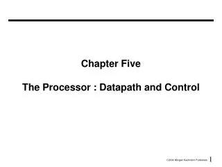
Goal: Design a Datapath
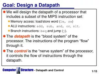
Goal: Design a Datapath. We will design the datapath of a processor that includes a subset of the MIPS instruction set: Memory access: load/store word ( lw, sw ) ALU instructions: add, sub, and, or , slt . Branch instructions: beq and jump ( j ).

Goal: Design a Datapath
E N D
Presentation Transcript
Goal: Design a Datapath • We will design the datapath of a processor that includes a subset of the MIPS instruction set: • Memory access: load/store word (lw, sw) • ALU instructions: add, sub, and, or, slt. • Branch instructions: beq and jump (j). • The datapath is the “blood system” of the processor. The instructions of the program “flow” through it. • The control is the “nerve system” of the processor, it controls the flow of instructions through the datapath. Computer Structure- Datapath and Control 1/15
Abstract View of the DataPath • The data path contains 2 types of logic elements: • Combinational: Elements whose outputs depend on their inputs. The ALU is an combinational element. • State: Elements with internal storage. (memory and registers). Computer Structure- Datapath and Control 2/15
A state element has at least two inputs and one output. The inputs are the data value to be written into the element and the clock signal which determines when the value will be written. The output is the data value stored in the element. Thus a state element can be read from at any time but written depending on the clock. • A clocking methodology defines when signals can be read and written. This is crucial (חיוני) to the correct design of a computer. • We will assume an edge-triggeredclocking methodology. Any values stored in the machine are updated only on a clock edge. • Because only state elements can store values, any collection of combinational logic must have its inputscoming from a set of state elements and its outputs written to set of state elements. The time necessary for the signals to reach element 2 defines the length of the clock cycle. Computer Structure- Datapath and Control
Edge-Triggered Clocking An edge-triggered clockallows us to read the contents of an register, send the value through some combinational logic and write that register in the same clock cycle. We assume that state elements have implicit clock signals. Computer Structure- Datapath and Control 3/15
Fetching an Instruction • An Instruction is read from memory and the PC is updated to point to the next instruction (4 is added). Computer Structure- Datapath and Control 4/15
For every instruction the first two steps are identical: • Fetch an instruction from where the PC points to in memory. • Decode the instruction and read the registers or memory contents specified. • A memory unit will hold the instructions that are to be executed. The address of the next instruction is in the PC. We need an ALU that performs only addition in order to calculate the next instruction to fetch, which is to add 4 (the length of an instruction) to the PC. • Thick arrows symbolize 32-bit buses (ערוצי מידע)unless specified differently. Thin arrows specify 1-bit lines, colored lines specify control lines. Computer Structure- Datapath and Control
The Register File • The fields of the instruction define which registers to read from and which to write to. • When the RegWrite line is set the result of the ALU is written into the register file. Computer Structure- Datapath and Control 5/15
The R-type instructions (also called the arithmetic-logical instructions) read the contents of 2 registers, perform an ALU op. , and write the result back into a third register. • The 32 registers are stored in the register file. The register file has 3 5-bit inputs to specify the registers, 2 32-bit outputs for the data read, 1 32-bit input for the data written and 1 control signal to decide if data should be written in. In addition we will need an ALU to perform the operations. Computer Structure- Datapath and Control
Data Memory • The contents of the base register are added to offset, this is the effective address, the address we will load from or store to. Computer Structure- Datapath and Control 6/15
The 2 elements needed to implement load and store instructions are data memory and a unit that sign-extends the 16-bit constant in an I-type instruction. This is necessary so the 16-bit immediate value can be used in a 32-bit ALU. • The existing ALU is used to compute the address to access. • The data memory has 2 32-bit inputs, the address and the write data, and 1 32-output: the read data. In addition it has 2 control lines: MemWrite and MemRead. MemWrite is set (set to 1) when a store is performed. MemRead is set when a load is performed. Computer Structure- Datapath and Control
Branch Equal Computer Structure- Datapath and Control 7/15
The beq instruction has 3 operands: two registers that are compared for equality and a 16-bit offset used to compute the branch address relative to the PC. To implement this instruction we must add the sign-extend offset to the PC. • There are 2 important details:1. The base for the address calculation is the address after the current instruction's address. But since we compute PC+4 when fetching we already have this address2. The offset is in words not bytes so we have to shift left the offset by 2. • Thus we have an ALU which performs the equality test and another ALU which performs the branch address computation. Computer Structure- Datapath and Control
Combined ALU and Memory Datapath • The ALU datapath and Memory datapath are similar. Why not combine them? Computer Structure- Datapath and Control 8/15
The ALU datapath (slide 6) and the Memory datapath (slide 7) are similar. The differences are: • The second input to the ALU is a register (R-type) or the sign-extended offset (I-type). • The value stored into the destination register comes from the ALU (R-type) or from memory (I-type) . • Using 2 multiplexors (Mux) we can combine both datapaths. • The next slide which shows a complete datapath can compute ALU instructions (add, sub, and, or, and slt), access memory (lw, sw), and compute the next instruction's address (beq, j). • All this is performed in a single cycle, from the moment the instruction is fetched until the next one is fetched only one machine cycle has passed. Computer Structure- Datapath and Control
A Single Cycle Datapath Computer Structure- Datapath and Control 9/15
Control in the Datapath • How does the processor "know” what operation to perform in the ALU? • How does the Data Memory "know" if to read, write, or do nothing? • The control (שליטה, בקרה) of the processor "commands" the units, through the control lines. • The fields of the instructions are the input to the control unit. Computer Structure- Datapath and Control 10/15
ALU Control • The operation of the ALU is definedby 2 fields of the instruction: • Opcode: The type of the instruction defines the ALU operation. Loads and stores need the ALU for addition (base register + offset). • Function: The operation of R-type instructions are set by the function field. • The ALU control defines the ALU operation: add, subtract, AND, OR, slt Computer Structure- Datapath and Control 11/15
ALU Control • The operation to be performed in the ALU depends on the opcode of the instruction, and on the function field of R-type instructions. • The ALU has 3 control inputs, we use 5 of the 8 possible input combinations, these are the outputs of the ALU control:000 AND001 OR010 add110 subtract111 slt • The ALU control uses as its inputs the funct field of the instruction and a 2-bit control field called the ALUOp. • For lw/sw the ALU computes the address using addition (ALUOp=00), for R-type instructions the ALU performs one of 5 actions depending on the function field of the instruction (ALUOp=10), for beq the ALU performs a subtraction (ALUOp=01). • Thus the load, store, anmd branch instructions don't need a function field, the operation is defined only from the opcode. • The ALU control is a large truth table that given the funct field and ALUOp outputs 3-bit controls for the ALU. Computer Structure- Datapath and Control
ALU Control Examples • The instruction fetched is beq $s0,$s1,L1: • What value is the ALUop? • What value is the ALU control output? • What are the ALU operands? • What is the ALU output? • Why doesn't beq need a function field? • The instruction fetched is slt $t0,$s0,s1: • Answer the previous asked questions? • Why does slt need a function field? Computer Structure- Datapath and Control 12/15
Main Control • Look at the formats of the R-type and I-type instructions:Field opcode rs rt rd shamt funct Bits 31-26 25-21 20-16 15-11 10-6 5-0Field opcode rs rt address Bits 31-26 25-21 20-16 15-0 • The following observations can be made: • The opcode is always in bits 31-26 • The 2 registers to be read are the rs and rt fields (R-type, beq, and store). • The base register for load/ store is always rs • The 16-bit offset for beq, lw,sw is always in bits (15-0) • The destination register is in: For a lw it is rt, for a R-type it is rd. A MUX selects which field of the instruction is written. Computer Structure- Datapath and Control 13/15
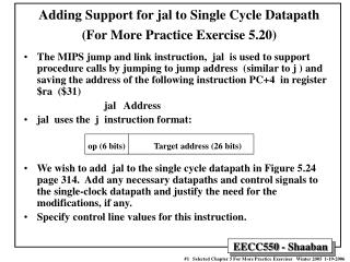
The Main Control Signals • The control signals are set by the type of instruction, by the opcode.There are 7 control signals in our microprocessor, let's see what happens when they are asserted (set to 1) and deasserted (set to 0):Signal Deasserted AssertedRegDst The Write reg is rt The Write reg is rdRegWrite None The Write register is written with the Write data ALUSrc The 2nd ALU operand The 2nd ALU operand is the comes from the register file is the 16-bit addressPCSrc PC=PC + 4 PC=Branch targetMemRead None Memory contents at the address input are put on the Read data outputMemWrite None Memory contents at the address input are replaced by the Write data inputMemtoReg The value of the reg. Write The value of the reg. Write data input is from the ALU data input is from memory Computer Structure- Datapath and Control
Main Control Diagram 14/15
Opcode to Control • The control lines are determined by the opcodes of the instructions. The exception is the PCSrc line which is dependent on the output of the beq instruction as well (x means don't care). • Line R-type lw sw beqRegDst 1 0 x xALUSrc 0 1 1 0MemtoReg 0 1 x xRegWrite 1 1 0 0MemRead 0 1 0 0MemWrite 0 0 1 0Branch 0 0 0 1ALUOp 10 00 00 01 • At this stage the Control is a block box, which receives inputs and gives outputs. Computer Structure- Datapath and Control 15/15