Download
1 / 49
510 likes | 784 Vues
The Silicon Vertex Detector of the Belle II Experiment . Thomas Bergauer ( HEPHY Vienna). 12th Pisa Meeting on Advanced Detectors. Belle and Belle II DEPFET Pixel Detector Double-sided Strip Detector Summary. Belle. KEKB. Linac. KEKB and Belle @ KEK (1999-2010).

E N D
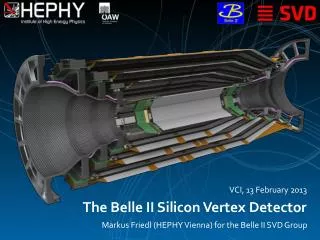
The Silicon Vertex Detector of the Belle II Experiment Thomas Bergauer (HEPHY Vienna) 12th Pisa Meeting on Advanced Detectors
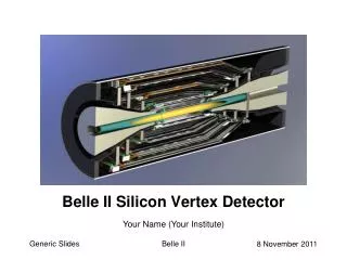
Belle and Belle IIDEPFETPixel DetectorDouble-sided Strip DetectorSummary Thomas Bergauer
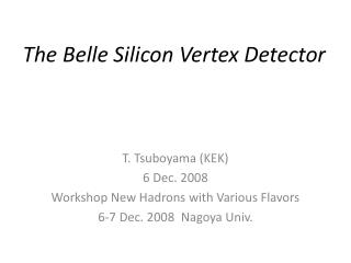
Belle KEKB Linac KEKB and Belle @ KEK (1999-2010) • Asymmetric machine:8 GeVe- on 3.5 GeVe+ Belle KEKB ~1 km in diameter Linac • Center of mass energy: Y(4S) (10.58 GeV) • High intensity beams (1.6 A & 1.3 A) • Integrated luminosity of 1 ab-1recorded in total • Belle mentioned explicitly in 2008 Physics Nobel Prize announcement to Kobayashi and Maskawa About 60km northeast of Tokyo Thomas Bergauer
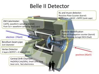
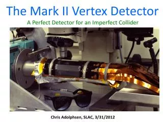
Belle Detector (1999–2010) Aerogel Cherenkov counter n=1.015~1.030 SC solenoid 1.5 T 3.5 GeV e+ CsI(Tl) 16 X0 TOF counter 8 GeV e- Central Drift Chamber small cell +He/C2H5 Si vertex detector 4 layers DSSD µ / KL detection 14/15 lyr. RPC+Fe Thomas Bergauer
SuperKEKB/Belle II Upgrade: 2010–2015 • Aim: super-high luminosity ~81035 cm-2s-1 11010 BB / year • LoI published in 2004; TDR published in 2010 • Refurbishment of accelerator and detector required • nano-beams with cross-sections of ~10 µm x 60 nm • 10 mm radius beam pipe at interaction region http://belle2.kek.jp Thomas Bergauer
Previous SVD Layout (until 2010) • 4 straight layers of 4" double-sided silicon detectors (DSSDs) • Outer radius ofr~8.8 cm • Up to three 4” sensors are daisy- chained and read out by one hybrid located outside of acceptance region (VA1 chip) Thomas Bergauer
Belle Silicon Vertex Detector (SVD) • Previous SVD limitations were • occupancy (currently ~10% in innermost layer)need faster shaping • dead time (currently ~3%)need faster readout and pipeline • Belle II needs detector with • high background tolerance • pipelined readout • robusttracking • low material budget in active volume Current SVD is not suitable for Belle II Thomas Bergauer
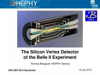
New Layout for Belle II SVD (2014-) • New double-layer pixel detector using DEPFET technology • Four layers with 6” double-sided strip detectors and forward part optimized for precision vertex reconstruction of the decays of short-lived B-mesons 4 layers of double-sided strip sensors Two layers of DEPFET pixels Thomas Bergauer
Belle and Belle IIDEPFET Pixel DetectorDouble-sided Strip DetectorSummary DEPFET PXD Posters: • Ultra-thin fully depleted DEPFET active pixel sensors for future e+/e- colliders– C. Koffmane • The DEPFET Active Pixels for Belle II - Resolution in 50 micron thinnedSensor – P. Kodys Thomas Bergauer
The DEPFET Belle-II PXD • Two layers mounted onto beam-pipe • Angular coverage 17°<θ < 155° • material budget below 0.5 % X0 • low power density of 0.1 W/cm2 • background occupancy to 1 - 3 % • z vertex resolution significantly improved (PXD & SVD) compared to Belle-I Thomas Bergauer
Self Supporting All-Silicon Module 3D Model of Belle-II Ladder Photo of thinned backside Material Budget Distribution: 0.19 %X0 in total Thomas Bergauer
DEPFET Sensors • DEPFET = depleted p-channel field effect transistor • Fully depleted sensitive volume • Charge collection in the “off” state, read out on demand • Modulation of the FET current by the charge in the internal gate • Clear contact to empty the internal gate Thomas Bergauer
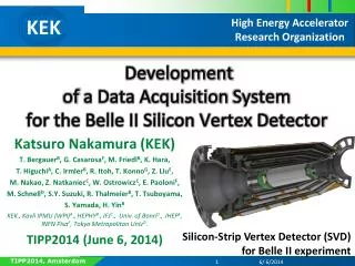
PXD Module Read-out • Switcher devices control the GATE and CLEAR (reset) lines • DCD (Drain Current Digitizer) is the readout chip with A/D converters • DHP (Digital Handling Processor) chips - first-stage preprocessing and data reduction • Belle II PXD produces huge data streams: raw 180 GB/s (20 PXD ladders, 8M pixels in total, occupancy up to 3%, trigger rate of 30kHz) • Data reduction necessary Thomas Bergauer
DEPFET/DCD-B Test System DCD-RO Line Driver and Buffer to FPGA DCD-B Read-out Chip Switcher-B for Clear and Gate Control PXD6 Belle-II DEPFET Matrix 32x64 Pixels L = 6 µm Pixel Size 50 x 50 µm² Thickness 50 µm 2nd Switcher-B Not used for Belle-II type PXD6 Design • 320 MHz DCD-B clock • 100 ns signal processing time per row Residuals distribution for perpendicular tracks with single pixel response (1) and more than 1 pixel response (2), σ=12 µm Thomas Bergauer
DAQ system of Belle II PXD • From DHP to DHH (Data Handling Hybrid) via 15m line: kapton converted to twisted-pair in a passive patch panel • DHHsvia optical links to ATCA Compute Nodes • ATCA CNsreduce data based on triggers • ATCA CNs compute fast tracking using SVD data to quickly identify regions of interest in the PXD Thomas Bergauer
Belle and Belle IIDEPFET Pixel DetectorDouble-sided Strip DetectorSummary Thomas Bergauer
SVD Configuration • Outermost layers 4-6 with slanted forward part (trapezoidal sensors) • Layer 3 with straight ladders: mechanics still under discussion • Sensors need to be read out individually (no daisy-chaining) • High background -> fast shaping time to keep occupancy low -> high noise -> short strips • However, very low material budget necessary Thomas Bergauer
Double-sided strip sensors from 6” wafer • Double sided strip silicon detectors with AC-coupled readout and poly-silicon resistor biasing made of 6 inch wafers • Size 12 x 6 cm • After market survey, prototypes ordered and delivered from • Hamamatsu (rectangular) • Micron (trapezoidal) Thomas Bergauer
Trapezoidal Sensors for Forward Region • Trapezoidal sensor for forward region • Different p-stop layouts on test sensors Atoll p-stop Common p-stop Combined p-stop Thomas Bergauer
Modules for Beam Test • Baby Modules used to verify p-stop layouts and geometries Trapezoidal Module Baby Module Thomas Bergauer
Stack Setup Two sensors for tracking (p-side) Two sensors for tracking (p-side) 120 GeVhadrons (mostly π) One module just forbalance Three DUTs, one of each p-stop pattern (n-side) Thomas Bergauer
Signal-to-noise-ratios • Dark colors: non-irradiated, Light colors: irradiated • Four geometries: width of „virtual“ strip defined by p-stop • Atoll pattern (half-wide) performs best, both irradiated and non-irradiated • Chosen for final sensor • Test sensors have been Gamma-irradiated with Co-60 (70 Mrad) • Tested before and after at CERN beam test (120 GeV hadrons) Thomas Bergauer
Eta Distributionsfor Atoll p-Stop Charge accumulation in unimplanted region Thomas Bergauer
Readout System Concept • Analog data transmission up to FADC by copper cable • Signal conditioning using FIR (Finite Impulse Response) filter • Prototype readout systemexists • Verified in several beam tests • Needs to be adapted for higher integration (chips/boards) FADC+PROC 1748APV25chips ~2mcoppercable Junctionbox ~10mcopper cable Unified opticaldata link (>20m) COPPER Front-endhybrids Rad-hardDC/DC converters Analog level translation,datasparsificationandhit time reconstruction Unified Belle IIDAQ system Thomas Bergauer
Prototypes 4A DC/DC converter prototype(developedat CERN) FADC+PROC (9U VME) Digitization, zero-suppression, hit time reconstruction Thomas Bergauer
Readout Chip: APV25 • Developed for CMS (LHC) by Imperial College London and Rutherford Appleton Lab • 70.000 chips installed • 0.25 µm CMOS process (>100 MRad tolerant) • 128 channels • 192 cell analog pipeline no dead time • 50 ns shaping time low occupancy • Multi-peak mode (read out several samples along shaping curve) • Noise: 250 e + 36 e/pF must minimize capacitive load!!! • Thinningto 100µm successful Thomas Bergauer
APV25 – Hit Time Reconstruction • Possibility of recording multiple samples (x) along shaped waveform (feature of APV25) • Reconstruction of peak time (and amplitude)by waveform fit • Offline now • Hardware later • Is used toremove off-timebackground hits Measurement Thomas Bergauer
Occupancy Reduction Belle -> Belle II Thomas Bergauer
Chip-on-Sensor Concept • Chip-on-sensor concept for double-sided readout • Flex fan-out pieces wrapped to opposite side (hence “Origami“) • All chips aligned on one side single cooling pipe Side View (below) Thomas Bergauer
Origami Module Assembly Ingredients: • DSSD sensors • Kapton PCB and pitch-adapters • APV Readout chips Followed by complicated assembly procedure • currently verified by all groups interested in ladder assembly Thomas Bergauer
Origami Module with 6” HPK DSSD Thomas Bergauer
Sketch of the Outermost Ladder (Layer 6) • Composed of 5 x 6” double-sided sensors • Center sensors have Origami structure • Averaged material budget over the full module: 0.55% X0 ca. 60cm Thomas Bergauer
Carried by ribs made of carbon fiber and Airex foam Very stiff, yet lightweight thanks to the sandwich construction Ladder Mechanics CO2 Cooling Pipe Sensor Support Ribs Thomas Bergauer
Belle and Belle IIDEPFET Pixel DetectorDouble-sided Strip DetectorSummary Thomas Bergauer
Summary • KEKBis the highest luminosity machine in the world • Upgradeof KEKB and Belle (2010-2015) • 40-fold increase in luminosity • Needs upgrades of all sub-detectors • New, enlarged Silicon Vertex Detector • Two layers of DEPFET pixels • Four double-sided strip layers • Strip Detector R&D • 6inch Double Sided Strip Detectors • Optimal p-stop geometry identified by SNR measurements before and after irradiation • Readout with hit time reconstruction for improved background tolerance • Origamichip-on-sensor concept for low-mass DSSD readout Thomas Bergauer
Advertisment http://vci.hephy.at Thomas Bergauer
Backup Slides follow The End. Thomas Bergauer
New IR with crab crossing and smaller by* Crab cavity 8GeV e- 3.5GeV e+ More RF for higher beam current New beam-pipes with ante-chamber Damping ring for e+ beam SR KEKB accelerator upgrade Thomas Bergauer
Faster calorimeter with waveform sampling and pure CsI (endcap) Background tolerant super small cell tracking detector Si vertex detector with high background tolerance (+2 layers, pixels) Belle-II KL/m detection with scintillator and next generation photon sensors New particle identifier with precise Cherenkov device: (i)TOP or fDIRC. Endcap: Aerogel RICH New dead-time-free pipelined readout and high speed computing systems Thomas Bergauer
Spatial Resolution of the Belle II Detector MC simulation for 50 and 75 mm thick silicon: intrinsic resolution in R-Fand Z • Extensive simulation study (ILC software framework): • To determine the expected Belle II PXD resolution • Cluster sizes • A/D conversion • Signal processing • Impact parameter • Vertex resolutions 75 mm thick silicon in R-F 50 mm thick silicon in R-F better resolution 75 mm thick silicon in Z 50 mm thick silicon in Z shift of the best resolution to 50 deg Thomas Bergauer
Sensor Types and Vendors Thomas Bergauer
Current Barrel Layout Origami Cooling Tubes Slanted Sensors Hybrid Boards Thomas Bergauer
Comparison VA1TA – APV25 VA1TA (SVD) • Commercial product (IDEAS) • Tp = 800ns (300 ns – 1000 ns) • no pipeline • <10 MHz readout • 20 Mrad radiation tolerance • noise: ENC = 180 e + 7.5 e/pF • time over threshold: ~2000 ns • single sample per trigger • APV25 (Belle-II SVD) • Developed for CMS by IC London and RAL • Tp = 50 ns (30 ns – 200 ns) • 192 cells analog pipeline • 40 MHz readout • >100 Mrad radiation tolerance • noise: ENC = 250 e + 36 e/pF • time over threshold: ~160 ns • multiple samples per trigger possible (Multi-Peak-Mode) Thomas Bergauer
Origami Module (TDC error subtracted) Measured Hit Time Precision • Results achieved in beam tests with several different types of Belle DSSD prototype modules (covering a broad range of SNR) • 2...3 ns RMSaccuracy at typical cluster SNR(15...25) • Working onimplementationin FPGA (using lookup tables) – simulationsuccessful Thomas Bergauer
Finite Impulse Response (FIR) Filter • Optimized channel • Non-optimized channel Raw APV25 output without FIR • FIR filter with 8 coefficients • Convolution (16-bit multiplications & sum) of incoming data at 40MHz Thomas Bergauer
Maximum Radiation Length Distribution APV Kapton Pipe Coolant Sensor CFRP Airex Thomas Bergauer
Cooling Boundary Conditions • Power dissipation per APV: 0.40 W • 1 Origamisensorfeatures 10 APVs • Total Origami power dissipation: 328 W • 360 W dissipated at the hybrid boards • Total SVD power dissipation: 688 W Thomas Bergauer
CO2Cooling • Closed CO2cooling plant underdevelopment • Collaborationwith CERN • First stepistogainexperiencewith open (blow) system Control cabinet with touch screen Accumulator 1.6 m 1.2 m 1.3 m Liquid pumps Thomas Bergauer