1 / 0

The Silicon Vertex Detector of the Belle II Experiment

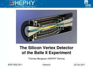
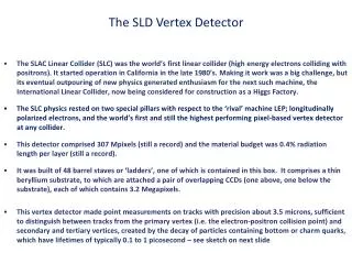
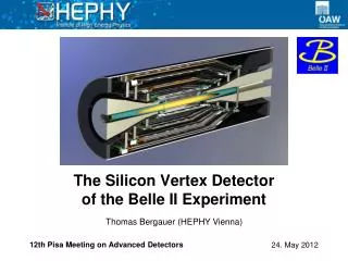
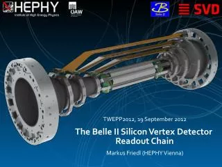
The Silicon Vertex Detector of the Belle II Experiment . Thomas Bergauer ( HEPHY Vienna). Vertex 2010. Loch Lomond. Introduction Belle II: The Future Double Sided Sensors SVD-II Components Readout System Summary. Mt. Tsukuba . Belle. Belle. KEKB. KEKB. ~1 km in diameter. Linac.

teddy
Télécharger la présentation

The Silicon Vertex Detector of the Belle II Experiment

An Image/Link below is provided (as is) to download presentation Download Policy: Content on the Website is provided to you AS IS for your information and personal use and may not be sold / licensed / shared on other websites without getting consent from its author. Content is provided to you AS IS for your information and personal use only. Download presentation by click this link. While downloading, if for some reason you are not able to download a presentation, the publisher may have deleted the file from their server. During download, if you can't get a presentation, the file might be deleted by the publisher.

E N D

Presentation Transcript


  1. The Silicon VertexDetectorof the Belle II Experiment

    Thomas Bergauer (HEPHY Vienna) Vertex 2010 Loch Lomond
  2. IntroductionBelle II: The FutureDouble Sided SensorsSVD-II ComponentsReadout SystemSummary T. Bergauer
  3. Mt. Tsukuba Belle Belle KEKB KEKB ~1 km in diameter Linac About 60km northeast of Tokyo Linac KEKB and Belle @ KEK Asymmetric machine:8 GeV e- on 3.5 GeV e+ Center of mass energy: Y(4S) (10.58 GeV) High intensity beams (1.6 A & 1.3 A) Integrated luminosity 1 ab-1 recorded by end of 2009 T. Bergauer
  4. Belle Detector (1999– 20. June 2010) Aerogel Cherenkov counter n=1.015~1.030 SC solenoid 1.5 T 3.5 GeV e+ CsI(Tl) 16 X0 TOF counter 8 GeV e- Central Drift Chamber small cell +He/C2H5 Si vertex detector 4 lyr. DSSD µ / KL detection 14/15 lyr. RPC+Fe T. Bergauer
  5. ThePresent SVD – Overview 4 layers (6/12/18/18 ladders), r = 2.0…8.8 cm 17°…150° polar angle coverage 246 double sided silicon detectors (DSSDs), 0.5 m2 overall active area VA1TA readout chip (Viking variant; 800ns shaping time) 110592 channels in total T. Bergauer
  6. IntroductionBelle II: The FutureDouble Sided SensorsSVD-II ComponentsReadout SystemSummary T. Bergauer
  7. KEKB/Belle upgrade (2010–2014) Aim: super-high luminosity ~81035 cm-2s-1 11010 BB / year LoI published in 2004; TDR was written in spring this year and is presently under review Refurbishment of accelerator and detector required http://belle2.kek.jp T. Bergauer
  8. Belle II SVD Upgrade (2010–2014) Ultimately 40-fold increase in luminosity (~81035 cm-2s-1) Present SVD limitations are occupancy (currently ~10% in innermost layer)need faster shaping dead time (currently ~3%)need faster readout and pipeline Needs Detector with high background tolerance pipelined readout robusttracking low material budget in active volume (low energy machine) Current SVD is not suitable for Belle II T. Bergauer
  9. Present SVD Layout (until 2010) 4 straight layers of 4" double-sided silicon detectors (DSSDs) Outer radius ofr~8.8 cm Up to 3 sensors are gangedand read out by one hybridlocated outside of acceptance T. Bergauer
  10. SVD-II Layout (2014-) Geometry optimization is underway New central pixel double-layer using DEPFET Strip layers extend to r~14 cm Every sensor is read out individually (no ganging) to maintain good S/N  chip-on-sensor concept 4 layers of double-sided strip sensors Double-layer of DEPFET pixels T. Bergauer
  11. IntroductionBelle II: The FutureDouble Sided SensorsSVD-II ComponentsReadout SystemSummary T. Bergauer
  12. Vendors for 6” DSSD Aim is to use double sided silicon detectors with AC-coupled readout and poly-silicon resistor biasing from 6 inch wafer Hamamatsu decided in the past to abandon the production of double sided sensors Thus, negotiations with Canberra, SINTEF and Micron started Finally HPK could be convinced to restart DSSD production on 6” wafers 6” prototypes ordered from Hamamatsu (rectangular): First batch delivered in April Micron (trapezoidal): First batch in July T. Bergauer
  13. SVD Layout Thomas Bergauer (HEPHY Vienna)
  14. First batch from HPK First 20 pieces of 6’’ sensors have been delivered in April 2010 Technical details: Dimensions: 59.6 x 124.88 mm p-side: Readout pitch: 75 µm 768 strips n-side: Readout pitch: 240 µm 512 readout strips n-side P-stop scheme T. Bergauer
  15. First Batch of 6” DSSD from HPK Electrical Characterization IV, CV Stripscan (p- and n-side) Longterm stability vs. temperature and humidity Inter-strip resistance and capacitance currently under investigation Pull-tests to show bondability ok T. Bergauer
  16. Trapezoidal Sensors (Micron) Full wafer designed using self-developed framework Including test structures and mini sensors to test different p-stop designs Delivery due July 2010 Trapezoidal sensor with test structures Sensor “programming language” T. Bergauer
  17. IntroductionBelle II: The FutureDouble Sided SensorsSVD-II ComponentsReadout SystemSummary T. Bergauer
  18. APV25 Readout Chip Developed for CMS (LHC) by IC London and RAL (70k chips installed) 0.25 µm CMOS process (>100 MRad tolerant) 40 MHz clock (adjustable), 128 channels 192 cell analog pipeline no dead time 50 ns shaping time low occupancy Noise: 250 e + 36 e/pF  must minimize capacitive load!!! Multi-peak mode (read out several samples along shaping curve) Thinning to 100µm successful Schematics of one channel T. Bergauer
  19. APV25 – Hit Time Reconstruction Possibility of recording multiple samples (x) along shaped waveform (feature of APV25) Reconstruction of peak time (and amplitude)by waveform fit Will be used toremove off-timebackground hits Measurement T. Bergauer
  20. Occupancy Reduction T. Bergauer
  21. Origami – Chip-on-Sensor Concept Chip-on-sensor concept for double-sided readout Flex fan-out pieces wrapped to opposite side (hence “Origami“) All chips aligned on one side  single cooling pipe Side View (below) Prototype for 4” DSSD (later with 6” sensors) T. Bergauer
  22. 4th Open Meeting of the Belle II Collaboration First Origami Module (2009) Top and bottom side Origami concept (4” sensor) Prototype completed in August 2009 Successfully evaluated in lab and beam tests Currently building module based on 6” sensor T. Bergauer 23
  23. Second Origami Module (2010) Now using new 6 inch sensors Kapton PCB and pitch-adapters ordered by Japanese company Currently under test in Vienna Followed by complicated assembly procedure T. Bergauer
  24. Sketch of the Outermost Ladder (Layer 6) Composed of 5 x 6” double-sided sensors Center sensors have Origami structure Border sensors are conventionally read out from sides ca. 60cm Cooling pipe Electronics for border sensor Structural element (CF) Flex circuits Connector (Nanonics) Electronics for border sensor T. Bergauer
  25. Carried by ribs made of carbon fiber and Rohacell Averaged material budget: 0.58% X0 Cooling options under study Conventional liquid cooling CO2 cooling Ladder Mechanics (preliminary) Cooling Pipe Sensor Support Ribs T. Bergauer
  26. IntroductionBelle II: The FutureDouble Sided SensorsSVD-II ComponentsReadout SystemSummary T. Bergauer
  27. Readout System Prototype readout systemexists Verified in several beam tests Basis for future SVD system shown below T. Bergauer
  28. Prototype Readout System Repeater Box Level translation, buffering FADC+PROC (9U VME) Digitization, zero-suppression, hit time reconstruction T. Bergauer
  29. Beam Tests KEK (Apr 2005) PSI (Aug 2005, Aug 2006) KEK (Nov 2007, Nov 2008) CERN (June 2008, September 2009) T. Bergauer
  30. IntroductionBelle II: The FutureDouble Sided SensorsSVD-II ComponentsReadout SystemSummary T. Bergauer
  31. Summary KEKB is the highest luminosity machine in the world Upgradeof KEKB and Belle (2010-2014) 40-fold increase in luminosity Needs upgrades of all subdetectors New, enlarged Silicon Vertex Detector DEPFETpixel double-layer Four strip layers Strip Detector R&D New 6” Double Sided Strip Detectors by HPK Origamichip-on-sensor concept for low-mass DSSD readout Readout with hit time reconstruction for improved background tolerance (up to 100x occupancy reduction w.r.t. now) T. Bergauer
  32. Backup Slides T. Bergauer
  33. Beam Parameters
  34. New IR with crab crossing and smaller by* Crab cavity 8GeV e- 3.5GeV e+ More RF for higher beam current New beam-pipes with ante-chamber Damping ring for e+ beam SR KEKB accelerator upgrade T. Bergauer
  35. Faster calorimeter with waveform sampling and pure CsI (endcap) Background tolerant super small cell tracking detector Si vertex detector with high background tolerance (+2 layers, pixels) Belle-II KL/m detection with scintillator and next generation photon sensors New particle identifier with precise Cherenkov device: (i)TOP or fDIRC. Endcap: Aerogel RICH New dead-time-free pipelined readout and high speed computing systems T. Bergauer
  36. Micron Wafer Layout 3 different GCDsfor the n-side Quadratic baby sensors 2,3,4 p-side: 512 strips 50 µm pitch 1 interm. strip n-side: 256 strips 100 µm pitch 0 interm. strip different p-stop patterns Main sensor p-side: 768 strips 75-50 µm pitch 1 interm. strip n-side: 512 strips 240 µm pitch 1 interm. strip combined p-stop Teststructures for p-side 1) atoll p-stop varying distance from strip 2) conventional p-stop varying width 3) combined p-stop varying distance from strip Baby sensor 1 p-side: 512 strips 50 µm pitch 1 interm. strip n-side: 512 strips 100 µm pitch 1 interm. strip atoll p-stop 1) 2) 3) Teststructures for n-side(no GCD) Thomas Bergauer (HEPHY Vienna)
  37. Micron: p-stop layout combined p-stops connected p-stops isolated Thomas Bergauer (HEPHY Vienna)
  38. Current Barrel Layout Origami Cooling Tubes Slanted Sensors Hybrid Boards T. Bergauer
  39. Comparison VA1TA – APV25 VA1TA (SVD) Commercial product (IDEAS) Tp = 800ns (300 ns – 1000 ns) no pipeline <10 MHz readout 20 Mrad radiation tolerance noise: ENC = 180 e + 7.5 e/pF time over threshold: ~2000 ns single sample per trigger APV25 (Belle-II SVD) Developed for CMS by IC London and RAL Tp = 50 ns (30 ns – 200 ns) 192 cells analog pipeline 40 MHz readout >100 Mrad radiation tolerance noise: ENC = 250 e + 36 e/pF time over threshold: ~160 ns multiple samples per trigger possible (Multi-Peak-Mode) T. Bergauer
  40. Origami Module (TDC error subtracted) Measured Hit Time Precision Results achieved in beam tests with several different types of Belle DSSD prototype modules (covering a broad range of SNR) 2...3 ns RMSaccuracy at typical cluster SNR(15...25) Working onimplementationin FPGA (using lookup tables) – simulationsuccessful T. Bergauer
  41. Origami Material Budget X0 comparison between conventional and chip-on-sensor (4” sensors): +50% increase in material, but also huge improvement in SNR Trade-off between material budget and SNR According to simulation, additional material is prohibitive in 2 innermost layers, but no problem for layers 3-5 OK with layout T. Bergauer
  42. Maximum Radiation Length Distribution APV Kapton Pipe Coolant Sensor CFRP Rohacell T. Bergauer
  43. Cooling Boundary Conditions Power dissipation/APV: 0.4 W 1 Origami sensor features 10 APVs Total Origami power dissipation: 356 W 404 W dissipated at the hybridboards Total SVD power dissipation: 760 W T. Bergauer
More Related