PCM4202 Questions
A customer measured the analog input resistance (Rin) of the PCM4202 at 6Kohm, while the datasheet states it should be 3Kohm. This discrepancy, highlighted by their test method, raises questions about the accuracy of the datasheet's measurement process. Additionally, the customer observed direct voltage readings of 5V and 0V on VIN+ and VIN-, respectively, conflicting with the datasheet description that the inputs are biased to VCC/2. Clarification on the measuring method and bias conditions is needed to ensure proper operation of the PCM4202.

PCM4202 Questions
E N D
Presentation Transcript
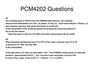
PCM4202 Questions Q1 Rin of Analog-input is 3Kohm from the PCM4202 data sheet p4, and customer measured the Rin(between Vin+/Vin-) by Tester* as Fig1-(c) , result shows 6Kohm ( 3Kohm x 2) and customer says that data sheet description is confirmed….. Is this reasonable? If No, would you please let us know the measuring method of Rin in the data sheet? * Note that power is ON (Vcc=5V/VDD=3.3V) when measuring the Rin by Tester Q2 When Customer had directly insert 5V or 0V as Fig1-(a)(b), customer seen 5V or 0V in the portion of VIN+ and also VIN- . Is this reasonable? In the data sheet p13, there are description that “The PCM4202 analog inputs are internally biased to approximately VCC/2.”,,, but Cusomer’s test result does not show that. In case of Fig-1-(a)(b), Vcom is Hi-Z ?? ( Fig2-(b) switch is OFF? )
VCC=5V VDD=3.3V VIN+ 5V 10K PCM4202 VIN- 5V is seen Fig1-(a) VCC=5V VDD=3.3V Fig1-(b) VIN+ 0V (GND) 10K PCM4202 Open Open VIN- 0V is seen Fig1-(c) VCC=5V VDD=3.3V Tester Tester shows “6kohm” VIN+ PCM4202 VIN-
Fig2-(a) Block Diagram(PCM4202D/S) Fig2-(b) Block Diagram (Customer’s Guess) Delta-Sigma Modulator VINR+ 3Kohm Switch ? Open 3Kohm VINR- VCOM=Vcc/2