Implementing a Counter and Parity Checking Circuit Using Finite State Machines
This guide explores the implementation of a counter and a parity-checking circuit utilizing finite state machines (FSMs). The counter counts sequentially through a defined range while the parity-checking circuit monitors an input for an odd or even number of 1s. The circuit design employs state transitions to manage input readings and output generation without the need for retaining all past inputs, thus optimizing performance. We will define states, create state diagrams, and establish the functions governing state transitions, ultimately enhancing your digital design skills.


Implementing a Counter and Parity Checking Circuit Using Finite State Machines
E N D
Presentation Transcript
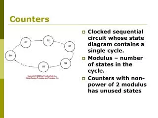
In class excercise • How to implement a “counter”, which will count as 0,3,1,4,5,7,0,3,1,……
Parity checking • Design a parity checking circuit that has one input X, and one output O. • X may change every clock cycle. The change happens at the falling edge. • The circuit samples the input at every rising edge of the clock. If the input is 1, consider as read a 1, else read a 0. • O is 1 if all the bits read so far contains an odd number of 1s and 0 otherwise.
Parity checking • Note that the output of the circuit depends on ALL past inputs. • So one possible implementation is to remember all past inputs. • Obviously bad…
Parity checking • A better implementation is to “summarize” the past inputs into some “states.” For what we are concerned about, • Knowing the current state, the value of the output can be uniquely determined. • Given the current state, the future state transition does not depend on the past inputs. • Note that • The states are just some binary numbers. • The number of states is significantly less than the number of input combinations, so we have a better circuit.
The difference from the counters • Counters also have states. For example, the state of the 3-bit counters are 0,1,2,3,4,5,6,7. • But counters have only the clk input, and is driven only by the clk. Knowing what the current state is, we know exactly what the next state should be. • Here, obviously, the next state also depends on the input X. • So we are moving to a more sophisticated example.
States • Finding out what the states should be is a bit of art. • Problems are different, so the solutions are also different. • Experience will help. • What the states of the parity checking circuit should be?
State • The state is the parity of the bits read so far. • Two states: S0 and S1. • S0: the bits have parity 0. • S1: the bits have parity 1.
State Diagram • The state transition diagram. • Draw a circle around the state. • Draw arrows from one state to another. • Beside the arrows, show the values of the inputs that caused this transition. X=1 S0 S1 X=1 X=0 X=0 X = 1 X = 0
Assign states • Need to assign binary number representations to the states. • Only one bit is needed. Let S0=0, S1=1.
Next State Function D = Q^X
Output function • The circuit should generate the output. • Clearly, the output function is O=Q.
Another FSM example – A sequence detector • One input X, and one output O. • X may change every clock cycle. The change happens at the falling edge. • The circuit samples the input at every rising edge of the clock. If the input is 1, consider as read a 1, else read a 0. • O is 1 (for one clock cycle, from positive edge to positive edge) if the last three bits read are 101.
Suggestions? • Do we need to remember any states? • What states do we need to remember?
Suggestions? • Maybe we just connect 3 Dffs and output 1 if Q2Q1Q0=101? • That is, we need to remember 8 states. • Can do better than that. • Remember what fractions of the sequence I have got.
4 states • S0: got nothing. The initial state. • S1: got 1. • S2: got 10. • S3: got 101. S0 S1 X=1 X=1 X=0 X=0 X=0 X=1 X=0 S3 S2 X=1 X = 1 X = 0
Assign states • S0 = 00 • S1 = 01 • S2 = 10 • S3 = 11
Next State Function D1 = (Q0&~X)|(Q1&~Q0&X) D0 = X
The output function • Clearly, O = Q1&Q0.