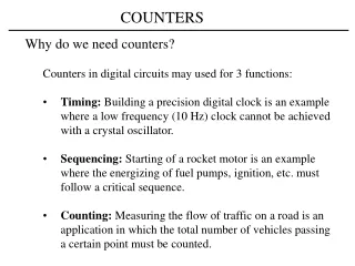
Counters
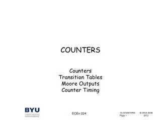
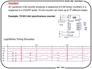
7. 1. P. 10. 163. 0. 1. T. 15. 0. 2. RCO. CLK. 6. 11. QD. QD. D. CLK. 5. 12. QC. C. QC. 4. 13. B. QB. QB. 3. 14. A. QA. QA. 9. 1. LOAD. 0. 1. 1. CLR. 0. CLR. Counters. An (up/down) k-bit counter produces a sequence of k-bit binary numbers in a

Counters
E N D
Presentation Transcript
7 1 P 10 163 0 1 T 15 0 2 RCO CLK 6 11 QD QD D CLK 5 12 QC C QC 4 13 B QB QB 3 14 A QA QA 9 1 LOAD 0 1 1 CLR 0 CLR Counters An (up/down) k-bit counter produces a sequence of k-bit binary numbers in a response to a COUNT pulse. A k-bit counter can have up to 2k different states Example: 74163 4-bit synchronous counter LogicWorks Timing Simulation 0 1 0 1 0 0 1 1 0 0 1 1 0 0 0 1
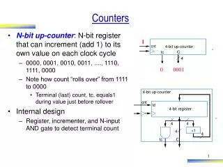
000 100 Present Next FF inputs C B A C+ B+ A+ TC TB TA 0 0 0 0 0 1 0 0 1 0 0 1 0 1 0 0 1 1 0 1 0 0 1 1 0 0 1 0 1 1 1 0 0 1 1 1 1 0 0 1 0 1 0 0 1 1 0 1 1 1 0 0 1 1 1 1 0 1 1 1 0 0 1 1 1 1 0 0 0 1 1 1 001 101 010 110 011 111 CB CB CB 00 01 11 10 00 01 11 10 00 01 11 10 A A A 0 0 0 1 1 1 Design of a 3-Bit Up-Counter Next-state Logic 1 1 1 1 0 0 0 0 0 0 0 0 1 1 1 1 1 1 1 1 0 1 1 0 TA=1 TB=A TC=AB
1 S S S 1 T Q T Q B T Q C A R R R Count \Reset 2 0 0 A B C C L K Design of a 3-Bit Up-Counter Flipflop input equations TA = 1 TB = A TC = AB 0 1 0 1 0 1 0 1 0 0 1 1 0 0 1 1 0 0 0 0 1 1 1 1
000 100 001 101 010 110 011 111 CB CB CB 00 01 11 10 00 01 11 10 00 01 11 10 A A A 0 0 0 1 1 1 Design of a 3-Bit Up-Counter Use D flipflops Present Next FF inputs C B A C+ B+ A+ DC DB DA 0 0 0 0 0 1 0 0 1 0 0 1 0 1 0 0 1 0 0 1 0 0 1 1 0 1 1 0 1 1 1 0 0 1 0 0 1 0 0 1 0 1 1 0 1 1 0 1 1 1 0 1 1 0 1 1 0 1 1 1 1 1 1 1 1 1 0 0 0 0 0 0 1 1 1 1 0 1 1 0 0 0 1 1 0 0 0 0 1 0 0 1 0 1 0 1 da = A db = Ab + aB dc = cB+cA+Cba
S D Q R da = A db = Ab + aB dc = cB+cA+Cba Up-Counter Using D Flipflops AB S S D Q B D Q C A R R Count \Reset T-FF realization is more efficient - requires less additional combinational logic
000 110 010 101 011 Complex-Counter Design Procedure 1. From specification, draw state-transition diagram to show the desired sequence to be realized by counter. 2. Choose flipflop type, then use FF excitation-table to derive next-state and FF-input equations. • Example: Design the following 5-state counter PS NS FF-inputs C B A C+ B+ A+ TC TB TA 0 0 0 0 1 0 0 1 0 0 0 1 X X X X X X 0 1 0 0 1 1 0 0 1 0 1 1 1 0 1 1 1 0 1 0 0 X X X X X X 1 0 1 1 1 0 0 1 1 1 1 0 0 0 0 1 1 0 1 1 1 X X X X X X Using K-maps: tc = Ac + aC tb = a + B + c ta = AbC + Bc Remark: The states that do not appear in the counter squence are treated as don’t care’s!
000 110 010 101 011 Self-Starting Counters In previous example, a problem may arise of the counter starts in one of the unused states (001, 100, or 111). Since these states were used as don’t-cares, then depending on how these don’t cares were used, counter may exhibit unwanted behavior. 111 000 001 110 001 010 100 101 011 111 100 Bad Design Counter may sequence through unwanted states forever (unless, reset). Better Design: If starts in an unwanted state, counter will go (atmost after one clock-cycle) into its normal state sequence.
PS NS FF-inputs C B A C+ B+ A+ TC TB TA 0 0 0 0 1 0 0 1 0 0 0 1 1 1 1 1 1 0 0 1 0 0 1 1 0 0 1 0 1 1 1 0 1 1 1 0 1 0 0 0 1 1 1 1 1 1 0 1 1 1 0 0 1 1 1 1 0 0 0 0 1 1 0 1 1 1 1 0 1 0 1 0 000 110 001 010 101 111 011 100 CB CB CB 00 01 11 10 00 01 11 10 00 01 11 10 A A A 0 0 0 1 1 1 Self-Starting Counters Another possible state diagram for a self-starting counter Next-state Logic 0 0 1 1 1 0 1 1 0 1 0 1 1 1 0 0 1 1 1 1 0 0 0 1 tc = Ac + aC tb = a + B + c ta = AbC + Bc
Q Q+ R S 0 0 X 0 0 1 0 1 1 0 1 0 1 1 0 X CB CB CB 00 01 11 10 00 01 11 10 00 01 11 10 A A A X X 1 X 0 0 1 X X 0 X X 0 0 0 X 0 X 0 X 1 X 0 X 0 X 1 1 1 1 CB CB CB 00 01 11 10 00 01 11 10 00 01 11 10 A A A 0 0 0 X 1 X 0 X 0 1 0 X 0 0 0 X 1 X X X 0 X 1 X X X 0 1 1 1 Counter Design with RS Flipflops • Example: Design the 5-state self-starting counter using RS flipflops PS NS FF-inputs C B A C+ B+ A+ RC SC RB SB RA SA 0 0 0 0 1 0 X 0 0 1 X 0 0 0 1 X X X X X X X X X 0 1 0 0 1 1 X 0 0 X 0 1 0 1 1 1 0 1 0 1 1 0 0 X 1 0 0 X X X X X X X X X 1 0 1 1 1 0 0 X 0 1 1 0 1 1 0 0 0 0 1 0 1 0 X 0 1 1 1 X X X X X X X X X RS-FF excitation table tc = A tb = ab+ac ta = c sc = a sb = B sa = bC
CB CB CB 00 01 11 10 00 01 11 10 00 01 11 10 A A A 0 0 X X 1 X X X 0 1 0 X 0 0 0 X 1 X X X X X 1 X X X X 1 1 1 CB CB CB 00 01 11 10 00 01 11 10 00 01 11 10 A A A X X 1 X X 0 1 X X X X X 0 0 0 X X X 0 X 1 X X X 0 X 1 1 1 1 Counter Design with JK Flipflops • Example: Design the 5-state self-starting counter using JK flipflops PS NS FF-inputs C B A C+ B+ A+ JC KC JB KB JA KA 0 0 0 0 1 0 0 X 1 X 0 X 0 0 1 X X X X X X X X X 0 1 0 0 1 1 0 X X 0 1 X 0 1 1 1 0 1 1 X X 1 X 0 1 0 0 X X X X X X X X X 1 0 1 1 1 0 X 0 1 X X 1 1 1 0 0 0 0 X 1 X 1 0 X 1 1 1 X X X X X X X X X JK-FF excitation table Q Q+ J K 0 0 0 X 0 1 1 X 1 0 X 1 1 1 X 0 jc = a jb = 1 ja = bC kc = A kb = a + c ka = C
1 0 C B A S S S 1 J J J Q Q Q C C C Q Q Q K K K R R R CLK RESET 1 0 Counter Design and Timing JK-FF Realization Timing Diagram
S=1 D3 Q3 D Q R S=1 D2 Q2 D Q R S=1 171 D1 Q1 D Q CLK Q3 R CLR Q2 S=1 D3 D0 Q0 D2 Q1 D Q D1 CLK R D0 Q0 CLR Storage Registers K-bit storage register can be realized by the parallel connection of K D-type flipflops RS or JK flipflops can be used instead as long as they implement the D-FF function! TTL 74171 package: Quadruple D-type Flipflop with Clear
171 377 CLK Q3 CLK CLR EN Q2 D3 D7 Q7 D2 Q1 D6 Q6 D1 D5 Q5 D0 Q0 D4 Q4 D3 Q3 D2 Q2 D1 Q1 D0 Q0 Data Bus 2:1 0 MUX 1 System Clock D 0 D 7 D 0 D 7 EN EN Select 74377 74377 Registers with Input Enable In the 74171, register contents may change with every positive clock edge. In the 74377, registers contents change (after the psoitive edge of CLK) only if EN is asserted (EN=0) • Potential use of 377 packages • in a computer system • Only one of the two 74377 • chips can READ from data • bus at a time,
Tri-State Buffers CLK 374 D7 Q7 CLK D6 Q6 H QH D5 Q5 G QG D4 Q4 F QF D3 Q3 E QE D2 Q2 D QD D1 Q1 C QC D0 Q0 B QB \OE A QA OE Data Bus 2:1 0 MUX 1 System Clock Q A Q H Q A Q H OE OE Select 74374 74374 Input Data Input Data Registers with Output Enables The 74374 8-bit register has tri-stated outputs, which are enabled by the OE input • Potential use of 374 packages • in a computer system • Only one of the two 74374 • chips can WRITE to data • bus at a time.
FF1 FF2 FF3 FF0 IN Q0 Q1 Q2 Q3 Serial input Serial output D Q D Q D Q D Q CLK Shift Registers 4-Bit Shift-register Correct Operation, assuming positive edge triggered FF 100 IN Q0 Q1 Q2 Q3 Clk
+ \RESET Q1 Q2 Q3 Q4 S S S S J Q J Q J Q J Q K K K K R R R R + \RESET Shift Registers Quad right-shift circular shift register using JK flipflops Shift When RESET=0, Q1 = 1, Q2 = Q3 = Q4 =0 Q1 Q2 Q3 Q4 \RESET = 1 1 0 0 0 \RESET = 0, Clk 0 1 0 0 \RESET = 0, Clk 0 0 1 0 \RESET = 0, Clk 0 0 0 1 \RESET = 0, Clk 1 0 0 0 \RESET = 0, Clk 0 1 0 0 . . . . . . . . . . . . . . . Also called Ring Counter
0 0 0 0 D Q D Q D Q D Q 1 1 1 1 S S S S Shift-Registers with Parallel Load IN.0 IN.1 IN.2 IN.3 2:1 MUX SI Q0 Q1 Q2 Q3 shift/L CLK SI = serial input Operation - following positive edges of CLK: if shift/L = 1 --> right-shift function is enabled (Q0 <-- SI, Qi <-- Qi-1) if shift/L = 0 --> parallel-load function is enabled (Qi <-- IN.i )
SRI SLI 0 0 0 0 D Q D Q D Q D Q 1 1 1 1 Q4 S S S S Q0 Q1 Q2 r/L Bidirectional Shift-Register Shift SRI: serial right input SLI: serial left input Operation - following positive edges of CLK: if r/L = 1 --> right-shift function is enabled (Q0 <-- SRI, Qi <-- Qi-1) if r/L = 0 --> left-shift function is enabled (Q4 <-- SLI, Qi <-- Qi+1)
FSMs are sequential machines that can have only a fixed number of states. Counters are FSMs in which the outputs and the states are identical In general the outputs and next states of an FSM are functions of the inputs and present states. The specification of output functions leads to two types of FSMs: Mealy machines: outputs are functions of inputs and present states Moore machines: outputs are functions of present states only Combinational logic for outputs and next-states Inputs X Outputs Z R CLK Combinational logic for next-states only State register Inputs X Comb. logic for outputs R Outputs Z CLK Finite State machine (FSM) Design Moore Machine Mealy Machine
Reset Even [0] PS input NS Output 0 0 0 0 0 1 1 0 1 0 1 1 1 1 0 1 0 1 1 Odd [1] 0 CLK = 1 2 3 4 5 6 7 8 9 10 IN = 0 1 0 1 1 0 0 1 1 0 OUT = 0 0 1 1 0 1 1 1 0 1 + S IN Q 1 D Q Example of input/ouput streams 0 C Q R Clk RESET Sequential Parity Checker Circuit that counts the 1’s in a bit-serial input stream. Odd-parity circuit: asserts its output when input stream contains an odd number of 1’s Even-parity circuit: asserts its output when input stream contains an even number of 1’s Odd-parity sequential machine State-transition table NS = PS xor IN OUT = PS Realization using a D-FF (a single T-FF can be used instead)
Design Procedure Understand problem input-output behavior define states Obtain an abstract representation of the FSM state diagrams, state tables Perform state minimization Perform state assignment:In an FSM with N=2n states, n state variables are needed to encode each state (i.e. each state is encoded by n bits) Choose flipflop types to implement the FSM: use flipflop excitation tables to derive the flipflop input equations. JK flipflops tend to reduce gate-count D flipflops tend to simplify design process Implement the FSM: use K-maps or Boolean logic to simplify next-state (or flipflop input) equations; simplify output equations Finite State machine Design
A Simple Vending Machine • Problem Statement: • Vending machine delivers a package of gum after receiving 15 cents in coins • Machine has a single coin slot and accepts nickels (N) and dimes only (D) • Machine does not give back change; inserting 2 dimes returns one package only Vending machine controller design Package Release Mechanism N Coin Sensor OPEN Vending Machine FSM D RESET CLK FSM must remember the total amount that has been received, and release a gum package when 15 cents (or 20) have been received. The machine sensor will reject any unknown coins
S0 [0 ¢] Reset N S1 [5 ¢] D N S2 [10¢] D N,D S3 [15¢] A Simple Vending Machine Constructing a state-diagram Possible states S0: initial (0 cents) state S1: received 5 cents S2: received 10 cents S3: received 15+ cents • State-Encoding: • The 4 states of the machine must be encoded • in binary. • Since we have four states, we need two bits to • encode each state (each bit is called a state-variable) Possible encodings State Q1 Q0 S0 0 0 S1 0 1 S2 1 0 S3 1 1 State Q1 Q0 S0 0 1 S1 1 1 S2 1 0 S3 0 0
PS inputs NS outputs Q1 Q0 D N Q1+ Q0+ OPEN 0 0 0 0 0 0 0 0 0 0 1 0 1 0 0 0 1 0 1 0 0 0 0 1 1 X X X 0 1 0 0 0 1 0 0 1 0 1 1 0 0 0 1 1 0 1 1 0 0 1 1 1 X X X 1 0 0 0 1 0 0 1 0 0 1 1 1 0 1 0 1 0 1 1 0 1 0 1 1 X X X 1 1 0 0 1 1 1 1 1 0 1 1 1 1 1 1 1 0 1 1 1 1 1 1 1 X X X Q1Q0 Q1 DN 0 0 1 1 0 1 1 1 N X X X X D 1 1 1 1 Q1 Q1Q0 Q1 DN 0 0 1 0 0 0 1 0 N X X X X D 0 0 1 0 Q1 A Simple Vending Machine D-FF implementation D1= Q1+, D0= Q0+ Q1Q0 Q1 DN 0 1 1 0 1 0 1 1 N X X X X D 0 1 1 1 Q1 K-Map for D1 K-Map for D0 d1 = q1 + d + nq0 d0 = nq1 + nQ0 + Nq0 + dq1 open = q1+ q0 K-Map for OPEN
Q1 D D1 D Q Q0 Q1 N \Q0 OPEN N Q0 N D Q Q1 Q0 D0 N Q1 D CLK \RESET Vending Machine FSM Implementation FSM Implementation with D flipflops (Moore machine) Flipflop (next-state) equations d1 = q1 + d + nq0 d0 = nq1 + nQ0 + Nq0 + dq1 open = q1+ q0
FSM Design for a Vending Machine JK-FF Implementation PS inputs NS FF outputs Q1 Q0 D N Q1+ Q0+ J1 K1 J0 K0 OPEN 0 0 0 0 0 0 0 X 0 X 0 0 0 0 1 0 1 0 X 1 X 0 0 0 1 0 1 0 1 X 0 X 0 0 0 1 1 X X X X X X X 0 1 0 0 0 1 0 X X 0 0 0 1 0 1 1 0 1 X X 1 0 0 1 1 0 1 1 1 X X 0 0 0 1 1 1 X X X X X X X 1 0 0 0 1 0 X 0 0 X 0 1 0 0 1 1 1 X 0 1 X 0 1 0 1 0 1 1 X 0 1 X 0 1 0 1 1 X X X X X X X 1 1 0 0 1 1 X 0 0 0 1 1 1 0 1 1 1 X 0 0 0 1 1 1 1 0 1 1 X 0 0 0 1 1 1 1 1 X X X X X X X j1 = d + nq0 k1 = 0 j0 = nQ0 + dq1 k0 = nQ1 open = q1+ q0
D J Q Q0 Q1 N K 0 OPEN \Q0 N J Q Q0 Q1 D K \Q1 N CLK \RESET Vending Machine FSM Implementation j1 = d + nq0 k1 = 0 j0 = nQ0 + dq1 k0 = nQ1 open = q1+ q0 FSM implementation with JK flipflops (Moore Machine)
ND/0 ND/0 S0 [0] S0 Reset Reset Reset/0 Reset/0 OPEN Reset/0 N/0 Reset N S1 [0] S1 ND ND/0 D D/0 N N/0 OPEN S2 [0] S2 D D/1 ND ND/0 D/1 N/1 N,D S3 [1] S3 Reset Reset/1 Moore and Mealy Machines: State Diagrams • Complete Moore machine state • diagram for vending machine • Outputs are associated • with states (graph nodes) • Complete Mealy machine state • diagram for vending machine • Outputs are associated with inputs • along transition arcs
PS inputs NS outputs Q1 Q0 D N Q1+ Q0+ OPEN 0 0 0 0 0 0 0 0 0 0 1 0 1 0 0 0 1 0 1 0 0 0 0 1 1 X X X 0 1 0 0 0 1 0 0 1 0 1 1 0 0 0 1 1 0 1 1 0 0 1 1 1 X X X 1 0 0 0 1 0 0 1 0 0 1 1 1 0 1 0 1 0 1 1 0 1 0 1 1 X X X 1 1 0 0 1 1 1 1 1 0 1 1 1 1 1 1 1 0 1 1 1 1 1 1 1 X X X PS inputs NS outputs Q1 Q0 D N Q1+ Q0+ OPEN 0 0 0 0 0 0 0 0 0 0 1 0 1 0 0 0 1 0 1 0 0 0 0 1 1 X X X 0 1 0 0 0 1 0 0 1 0 1 1 0 0 0 1 1 0 1 1 0 0 1 1 1 X X X 1 0 0 0 1 0 0 1 0 0 1 1 1 1 1 0 1 0 1 1 1 1 0 1 1 X X X 1 1 0 0 1 1 1 1 1 0 1 1 1 1 1 1 1 0 1 1 1 1 1 1 1 X X X Moore and Mealy Machines: State Tables Vending Machine Example S0 S0 S1 S1 S2 S2 S3 S3 Moore machine state table Outputs are associated with states (graph nodes) Mealy machine state table Outputs are change with inputs
0 S0 (Z=0) S1 (0) S2 (1) 1 1 W=0 1 0 Binary string Recognizers Example: Construct an FSM that receives a bit-serial binary input W and asserts its output Z whenever its input string has at least two 1’s in sequence. Solution: (1,a) - Input-output behavior CLK 1 2 3 4 5 6 7 8 9 A B C D W 0 1 0 1 1 1 0 1 1 1 1 0 0 Z 0 0 0 0 1 1 0 0 1 1 1 0 0 (1.b) - Define states (Moore model) S0: received 0 (most recently) Z=0 S1: received 1 (most recently) Z=0 S2: received two 1’s in sequence Z=1 (2) - State diagram (Moore model)
D1 State Q1 Q0 S0 0 0 S1 0 1 S2 1 1 Z D Q Q1 CLK R D Q W Q0 D0 CLK R PS IN NS OUT FF Q1 Q0 W Q1+ Q0+ Z D1 D0 0 0 0 0 0 0 0 0 0 0 1 0 1 0 0 1 0 1 0 0 0 0 0 0 0 1 1 1 1 0 1 1 1 0 0 x x x x x 1 0 1 x x x x x 1 1 0 0 0 1 0 0 1 1 1 1 1 1 1 1 Binary string Recognizers Example: Binary string recognizer (3) - State assignment: 3 states means that we need two bits to represent each state d1 = wq0 d0 = wq0 + wQ1 z = q1
1/1 S0 S1 1/0 0/0 W=0/Z=0 Z W D Q CLK \RESET Binary string Recognizers • Example: Binary string recognizer • (1.b) - Define states (Mealy model) • S0: received 0 (most recently) • S1: received at least one 1 (most recently) • (2) - State diagram (Mealy model) • (3) - State assignment • (S0 := 0 , S1 := 1) PS IN NS OUT Q W Q+ Z D T J K 0 0 0 0 0 0 0 X 0 1 1 0 1 1 1 X 1 0 0 0 0 1 X 1 1 1 1 1 1 0 X 0 Output Z=WQ D-FF: D=W T-FF: T=W xor Q JK-FF: J=W K=W
J Q X A ja = x ka = xB jb = x kb = x A z = b \B K X J X Q Z=B K \A X CLK \RESET AB AB 00 01 11 10 00 01 11 10 X X K-map for A+ K-map for B+ 0 0 0 1 1 0 0 0 1 0 1 1 1 1 0 1 1 1 0 1 Analysis of FSMs Problem Given the hardware schematic of a sequential machine, determine its state behavior and output functions. Example: Analyze the following sequential circuit Solution: 1- Find JK input equations 2- Compute next-state equations a+ = ja A + Ka a = xA + (X+b)a b+ = jb B + Kb b = xB + (XA+Xa)b
AB 00 01 11 10 X K-map for A+ 0 0 0 1 1 1 1 1 1 0 AB 00 01 11 10 X K-map for B+ 0 0 0 1 0 1 1 1 0 1 S0 Z=0 S3 Z=1 X=0 X=1 0 1 0 1 S1 Z=1 S2 Z=0 1 0 FSM Analysis A B X A+ B+ Z (=B) 0 0 0 0 0 0 0 0 1 1 1 0 0 1 0 0 0 1 0 1 1 1 1 1 1 0 0 1 0 0 1 0 1 0 1 0 1 1 0 1 1 1 1 1 1 1 0 1 S0 S1 S2 S3 More Machine: output isf function of present state only, Z=B
Z Clock cycle 4 3 2 1 1 0 0 1 1 1 1 0 SUM A 0 1 0 1 0 0 0 1 B 0 0 1 0 C Next state 1 S Q D Present state Q C R CLK \CLR Sequential (Bit-Serial) Adder Design Sequential adder operation to add two numbers A=ak ak-1 . . . a1 a0 and B=bk bk-1 . . . b1 b0 - start by adding a0 and a0 - output sum bit s0 and store carry bit c0 so that it is added to bits a1 and b1 in the next clock cycle - repeat the procedure for bits ai and bi (output si and store carry bit ci) Direct Design Implement design using a combinational logic block that generates next-state and output functions, and a storage element (D-FF) to store present state LSB Mealy Model
AB 00 01 11 10 Q K-map for J 0 0 0 1 0 1 X X X X AB 00 01 11 10 Q K-map for K 0 X X X X 1 1 0 0 0 Sequential Adder Design using Formal Methods AB=11/Z=0 01/0 10/0 11/1 Inputs: A, B Output: Z=SUM States (last carry bit): S0: carry was 0 S1: carry was 1 RESET S0 S1 00/0 01/1 10/1 00/1 PS IN NS OUT FF Q A B Q+ Z D J K 0 0 0 0 0 0 0 x 0 0 1 0 1 0 0 x 0 1 0 0 1 0 0 x 0 1 1 1 0 0 1 x 1 0 0 0 1 1 x 1 1 0 1 1 0 1 x 0 1 1 0 1 0 1 x 0 1 1 1 1 1 1 x 0 Z = A xor B xor Q D= Q j = ab k = AB
00 01 10 11 S0 Z=0 S2 Z=0 RESET 11 01 10 00 01 10 11 00 S0 Z=0 S2 Z=0 00 01 10 11 Moore Machine Realization of Sequential Adder More states are required for Moore Model S0: C=0 and Z=0 (C=carry, Z:sum) S1: C=0 and Z=1 S2: C=1 and Z=0 S3: C=1 and Z=1 State Diagram Two flipflops are needed to implement the Moore Model sequential adder Ex.: Implement this state diagram using D, flipflops and JK flipflops