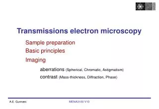
Transmissions electron microscopy
Transmissions electron microscopy. Basic principles Sample preparation Imaging aberrations (Spherical, Chromatic, Astigmatism) contrast (Mass-thickness, Diffraction, Phase). Project report. Report due Monday May 11, 14.00 Project presentation and oral ”exam” Friday May 15

Transmissions electron microscopy
E N D
Presentation Transcript
Transmissions electron microscopy Basic principles Sample preparation Imaging aberrations (Spherical, Chromatic, Astigmatism) contrast (Mass-thickness, Diffraction, Phase)
Project report • Report due Monday May 11, 14.00 • Project presentation and oral ”exam” Friday May 15 • Possible report outline: • Introduction about the material and motivation • Experimental methods used • Results and discussion • Conlusions • References
Basic principles, first TEM Wave length of electrons: 200kV: λ= 0.00251 nm (v/c= 0.6953, m/m0= 1.3914) Electrons are deflected by both electrostatic and magnetic fields Force from an electrostatic field F= -e E Force from amagnetic field F= -e (v x B) • The first electron microscope built by Knoll • and Ruska in 1933, b) The first commercial • electron microscope built by Siemens in 1939. Ernst Ruska: Nobel Prize in physics 1986
Basic TEM Electron gun Electron source: ●Tungsten, W ● LaB6 ● FEG Cold trap Sample position • Vacuum requirements: • Avoid scattering from residual gas in • the column. • - Thermal and chemical stability of the • gun during operation. • - Reduce beam-induced contamination • of the sample. • LaB6: 10-7 torr • FEG: 10-10 torr
The lenses in a TEM Filament Anode The diffraction limit on resolution is given by the Raleigh criterion: δd=0.61λ/μsinα, μ=1, sinα~ α 1. and 2. condenser lenses Sample Objective lens Compared to the lenses in an optical microscope they are very poor! The point resolution in a TEM is limited by the aberrations of the lenses. Intermediate lenses Projector lens • Spherical • Chromatic • Astigmatism
r2 r1 α Disk of least confusion Spherical aberrations r2 • Spherical aberration coefficient r1 α ds = 0.5MCsα3 M: magnification Cs :Spherical aberration coefficient α: angular aperture/ angular deviation from optical axis 2000FX: Cs= 2.3 mm 2010F: Cs= 0.5 nm
v - Δv v Chromatic aberration Disk of least confusion Chromatic aberration coefficient: dc = Ccα ((ΔU/U)2+ (2ΔI/I)2 + (ΔE/E)2)0.5 Cc: Chromatic aberration coefficient α: angular divergence of the beam U: acceleration voltage I: Current in the windings of the objective lens E: Energy of the electrons 2000FX: Cc= 2.2 mm 2010F: Cc= 1.0 mm Thermally emitted electrons: ΔE/E=kT/eU Force from amagnetic field: F= -e (v x B)
x y-focus y x-focus Lens astigmatism • Lens astigmatism Loss of axial asymmetry This astigmatism can not be prevented, but it can be corrected!
Resolution limit http://www.sfc.fr/Material/hrst.mit.edu/hrs/materials/public/ElecMicr.htm
Technical data of different sources http://dissertations.ub.rug.nl/FILES/faculties/science/1999/h.b.groen/c1.pdf H.B. Groen et al., Phil. Mag. A, 79, p 2083, 1999
Sample preparation for TEM Plane view or cross section sample? Is your material brittle or ductile? Is it a conductor or insulator? Is it a multi layered material? • Samples need to be ~100 nm thick. How? • Crushing • Cutting • saw, diamond pen, ultrasonic drill, FIB • Mechanical thinning • Grinding, dimpling • Electrochemical thinning • Ion milling • Coating • Replica methods
TEM sample preparation: Thin films Grind down/ dimple Cut out cylinder • Top view Ion beam thinning Grind down and glue on Cu-rings Cut out a cylinder and glue it in a Cu-tube Cut out slices • Cross section Glue the interface of interest face to face together with support material or • Focused Ion Beam (FIB) Cut a slice of the cylinder and grind it down / dimple Cut off excess material Ion beam thinning
BiFeO3 Pt TiO2 Glue SiO2 Si 200 nm Imaging / microscopy TEM - High resolution (HREM) - Bright field (BF) - Dark field (DF) - Shadow imaging (SAD+DF+BF) STEM - Z-contrast (HAADF) - Elemental mapping (EDS and EELS) GIF - Energy filtering Holography – Map magnetic domains – Map electrostatic potential – Enhance resolution
Apertures Condenser aperture Objective aperture Selected area aperture
3,8 Å 1,1 nm Simplified ray diagram Parallel incoming electron beam Si Sample Objective lense Diffraction plane (back focal plane) Objective aperture Selected area aperture Image plane MENA3100 V08
Use of apertures Condenser aperture: Limits the number of electrons hitting the sample (reducing the intensity), Reducing the diameter of the discs in the convergent electron diffraction pattern. Selected area aperture: Allows only electrons going through an area on the sample that is limited by the SAD aperture to contribute to the diffraction pattern (SAD pattern). Objective aperture: Allows certain reflections to contribute to the image. Increases the contrast in the image. Bright field imaging (central beam, 000), Dark field imaging (one reflection, g), High resolution Images (several reflections from a zone axis).
50 nm Objective aperture: Contrast enhancement Ag and Pb Si hole glue (light elements) A small aperture allows only electrons in the central spot in the back focal plane to contribute to the image. All electrons contribute to the image. Intensity: Thickness and density dependence Mass-thickness contrast Diffraction contrast (Amplitude contrast) One grain seen along a low index zone axis.
Objective aperture BF image Weak-beam DF image Diffraction contrast: Bright field (BF), dark field (DF) and weak-beam (WB) Dissociation of pure screw dislocation In Ni3Al, Meng and Preston, J. Mater. Scicence, 35, p. 821-828, 2000.
sample Obj. lens Obj. aperture BF image DF image DF image Bending contours
BF image DF image Thickness fringes, bright and dark field images Sample Sample
HREM image 2 nm Phase contrast: HREM and Moiré fringes Long-Wei Yin et al., Materials Letters, 52, p.187-191 A Moiré pattern is an interference pattern created, for example, when two grids are overlaid at an angle, or when they have slightly different mesh sizes (rotational and parallel Moire’ patterns). Interference pattern http://www.mathematik.com/Moire/ 200-400 kV TEMs are most commonly used for HREM
Moire’ fringe spacing Parallel Moire’ spacing dmoire’= 1 / IΔgI = 1 / Ig1-g2I = d1d2/Id1-d2I Rotational Moire’ spacing dmoire’= 1 / IΔgI = 1 / Ig1-g2I ~1/gβ = d/β Parallel and rotational Moire’ spacing dmoire’= d1d2/((d1-d2)2 + d1d2β2)0.5 g1 g2 Δg g1 Δg β g2