Programmable logic devices
Learn about the structure and functions of PLAs and Programmable Logic Devices (PLDs) in digital circuits. Dive into diode logic, Field-Programmable Arrays (FPGA), and more options in programmable devices.

Programmable logic devices
E N D
Presentation Transcript
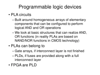
Programmable logic devices • PLA circuits • Built around homogeneous arrays of elementary components that can be configured to perform logical AND and OR operations • We look at basic structures that can realize AND, OR functions (in reality PLAs are based on NAND/NOR functions in CMOS technology) • PLAs can belong to • Gate arrays, if interconnect layer is not finished • PLDs, if fuses are provided along with a full interconnect layer • FPGA are PLD
Diode logic ( in the compact form, X indicates presence of a diode )
Diode logic • Multiple functions realized by an AND-OR array • ab is “shared” by both outputs
Diode logic • Example: • PLA table: • AND array: • 0 complement connected; • 1 true form connected; • X no connection • OR array: • 1 connection; • 0 no connection
Diode logic • Resulting PLA: • The AND and the OR arrays are programmable
a figure Diode logic How many literals in each prime implicant?
Field-programmable arrays • Uncommitted AND/OR arrays with metal fuses that can be blown. • Unprogrammed AND array:
Programmed AND function A’BC’ and its compact notation • X means fuse intact (not blown)
Fuse-programmable OR arrays • Unprogrammed: • Programmed OR function P1+P3 and its compact notation
Other options in programmable devices • Output polarity options • Programmed active high • Programmed active low
Other options in programmable devices • Bidirectional pins and feedback lines • Driver enabled • Driver disabled
Other options in programmable devices • Bidirectional pins and feedback lines • When driver enabled, sum term Sm available as output and fed back to the AND array • This allows multilevel circuits (more than 2 levels) • When driver disabled, the IOm pin acts as external input • Example: implement a 2-bit ripple-carry adder • Use PLA with 4 inputs, 3 outputs and 2 bi-directional pins • Use one bi-directional pin for input, the other for output/feedback
Two-bit ripple carry adder implementation • Question: why are all the fuses left intact on product term 16?
Commercial PLDs • Basic PLD organization
Commercial PLDs • Some commercially available PLDs