Download
1 / 31
310 likes | 455 Vues
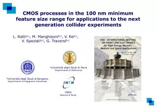
CMOS technologies in the 100 nm range for rad-hard front-end electronics in future collider experiments. V. Re a,c , L. Gaioni b,c , M. Manghisoni a,c , L. Ratti b,c , V. Speziali b,c , G. Traversi a,c. b Università degli Studi di Pavia Dipartimento di Elettronica.

E N D
CMOS technologies in the 100 nm range for rad-hard front-end electronics in future collider experiments V. Rea,c, L. Gaionib,c, M. Manghisonia,c, L. Rattib,c, V. Spezialib,c, G. Traversia,c bUniversità degli Studi di Pavia Dipartimento di Elettronica aUniversità degli Studi di Bergamo Dipartimento di Ingegneria Industriale cINFN Sezione di Pavia
Motivation Future generation of HEP experiments (LHC upgrade, ILC, Super B-Factory): mixed signal integrated circuits for the readout of silicon pixel and microstrip detectors designed in 130 nm (90 nm) CMOS processes Industrial technology development is driven by digital circuits; the critical aspects for detector readout chips are noise performance, power dissipation and radiation damage Inner SLHC detectors: ultra-deep submicron systems exposed to ionizing radiation doses of 100 Mrad and beyond While the scaling of the gate oxide thickness to about 2 nm gives a high degree of radiation tolerance, issues such as the gate tunneling current and the sidewall leakage associated to lateral isolation oxides must be investigated. With special focus on the design of analog front-end circuits for silicon pixel and strip detectors, the impact of ionizing radiation on the noise performance is evaluated and the underlying physical degradation mechanisms are pointed out to provide criteria for improving radiation hardness properties. Sensitivity to Single Event Effects (SEE) can be a major problem for digital systems in 100-nm scale CMOS. The discussion of SEE and of circuit design for SEE immunity is beyond the scope of this talk.
Technology features: VDD = 1.2 V Physical oxide thickness tOX= 2 nm COX=15 fF/μm2 G S D Leakage path G D S Standard Enclosed Investigated technologies and devices Standard open layout PMOS and NMOS transistors from HCMOS9 130 nm and CMOS090 90 nm triple well, epitaxial CMOS technologies by STMicroelectronics HCMOS9 (Lmin=130 nm) CMOS090 (Lmin=90 nm) Technology features: • VDD = 1 V • Physical oxide thickness tOX= 1.6 nm • COX=18 fF/μm2 Enclosed layout NMOS transistors (and standard PMOS) from 2nd130 nm CMOS vendor (CERN)
Irradiation tests Front-end integrated circuits for inner detectors at SLHC must feature a high radiation resistance, up to several hundred Mrad total dose of ionizing radiation. Outer SLHC detector layers and less demanding (in terms of rad-hard requirements) collider experiments set radiation tolerance specifications of several Mrad on front-end electronics 10 Mrad irradiation 100 Mrad irradiation 60Co g-rays • 90 nm and 130 nm open layout devices from STMicroelectronics 10 keV X-rays • PMOS and enclosed NMOS from 2nd 130 nm vendor 10 keV X-rays • 90 nm open layout devices from STMicroelectronics • PMOS and enclosed NMOS from 2nd 130 nm vendor The MOSFETs were biased during irradiation in the worst-case condition (all terminals grounded, except gate of NMOS kept at VDD)
Ionizing radiation effects and scaling of the gate oxide thickness in ultra deep submicron CMOS In very thin gate oxides (2 nm), radiation induced positive trapped charge is removed by tunneling processes Effects on threshold voltage and static drain current characteristics are very small; threshold voltage shift at 100 Mrad is of the order of 1 mV, if any In PMOSFETs and in enclosed 130 nm NMOSFETs, Id vs Vgs curves are unaffected by irradiation.
Radiation effects in open layout NMOS Radiation induced increase of the drain current is apparent in the constant leakage current zone and in the subthreshold region. This effect is larger in the 130 nm devices, whereas the impact is minor in 90 nm transistors. This behavior is associated to the lateral parasitic transistors at the edge of the device.
Radiation effects in lateral isolation structures In deep submicron bulk CMOS devices exposed to ionizing radiation, the main degradation effects are associated to the thick (~ 300 nm) lateral isolation oxides (STI = Shallow Trench Isolation). Radiation-induced positive charge trapped in isolation oxides may invert a P-type region in the well/substrate of NMOSFETs creating a leakage path between source and drain.
Radiation effects in lateral isolation structures Lateral parasitic transistors turn on because of charge build up in STI oxides. N+ Drain Source-drain leakage paths Gate Poly The parasitic devices add a contribution to the total drain current and noise of NMOSFETs. Source N+ STI We developed a model to account for the white and 1/f noise degradation due to the effect of lateral parasitic transistors. Main transistor finger V. Re et al, “Impact of lateral isolation oxides on radiation-induced noise degradation in CMOS technologies in the 100 nm regime”, NSREC ‘07 Lateral parasitic devices
Radiation effects in lateral isolation structures For devices with a large W/L ratio (no narrow channel effect) the total contribution from lateral devices can be disentangled from the drain current of the main transistor controlled by the gate oxide. The impact of lateral parasitic devices is larger at small current densities ID. L/W
Radiation effects in lateral isolation structures The drain current is more severely affected by sidewall leakage in the 130 nm technology as compared to the 90 nm one. This could be explained by a higher doping concentration in the p-type body for the 90 nm process, which mitigates the inversion of the surface along the STI sidewalls.
Radiation effects on noise Signal-to-noise ratio is a critical issue for the design of silicon tracking and vertexing detectors. Noise vs power performance and radiation effects on noise are crucial parameters for the choice of the technology for integrated front-end electronics, especially in view of operating with thin and/or heavily irradiated silicon detectors, where the collected charge will be considerably smaller than for standard 300 mm sensors. In 100-nm scale open layout CMOS devices, 1/f noise at small drain current density is among the few parameters which are sensitive to ionizing radiation.
Radiation effects on noise Noise in the drain current of a MOSFET can be represented through an equivalent noise voltage source in series with the device gate SW - white noise • channel thermal noise (main contribution in the considered operating conditions) • other contributions from parasitic resistances S1/f - 1/f noise • technology dependent contribution • both kf and αf depend on the polarity of the DUT • kf 1/f noise parameter • αf 1/f noise slope-related coefficient • kB Boltzmann’s constant • T absolute temperature • αw excess noise coefficient • γ channel thermal noise coefficient
Radiation effects on noise: NMOS 90 nm In 90 nm open layout NMOSFETs, at 10 Mrad total dose the main radiation effect is a 1/f noise increase at low current density, due to the contribution of lateral parasitic devices. No increase in the white noise region is detected.
Radiation effects on noise: NMOS 90 nm At 100 Mrad, there is no sizable difference in radiation effects with respect to 10 Mrad. A further increase of 1/f noise is detected.
Radiation effects on noise: NMOS 130 nm open layout In 130 nm open layout NMOSFETs, at 10 Mrad total dose the main radiation effect is again a 1/f noise increase at low current density, due to the contribution of lateral parasitic devices. Since the impact of lateral devices is larger for this process, a noise increase in the white spectral region is also detected at low currents.
Radiation effects on noise: NMOS 130 nm enclosed In 130 nm enclosed NMOSFETs, at 100 Mrad total dose, noise degradation is negligible. This provides evidence for a model where the basic mechanism underlying noise increase in irradiated devices is associated to lateral parasitic transistors.
Radiation effects on noise: PMOS In 130 nm and 90 nm PMOS (open layout), even at 100 Mrad total dose, noise degradation is negligible. This is in agreement with the absence of sidewall leakage current contributions.
1/f noise coefficient Kf At 100 Mrad total dose, Kf is very close to preirradiation values for enclosed NMOS and for PMOS. Instead, Kf sizably increases at low drain current density for open layout NMOS. NMOS open layout NMOS enclosed, PMOS
Ionizing radiation effects on the gate leakage current The absorption of a 100 Mrad total dose marginally affects the gate leakage current (mostly due to direct tunneling through the thin gate oxide). However, there may be reliability problems (hard oxide breakdown) to be investigated.
Thick oxide I/O devices In 90 nm CMOS, the gate current due to tunneling effects may play a sizable role affecting the signal-to-noise ratio of a front-end system, especially at peaking times above 100 ns. To avoid this problem, we could use devices with thicker gate oxide and higher VDD available in advanced CMOS technologies. However, a thicker gate oxide may give worse noise performances and is more sensitive to ionizing radiation. Preliminary tests on the STM 90 nm process show that I/O 2.5 V NMOSFETs have a 1/f noise parameter Kf 20 times bigger than standard core transistors with thin oxide.
Low noise charge preamplifier design Circuit designers can take advantage of single device characterization to predict noise behavior of charge sensitive amplifiers Equivalent noise charge is the figure of merit to be minimized: • CD detector capacitance • CG preamplifier input capacitance • tp peaking time • A1 A2 shaping coefficients Flicker noise contribution Channel thermal noise contribution Data extracted from single transistor characterization can be used to plot minimum ENC as a function of the main design parameters (peaking time, power dissipation, polarity and dimensions of the preamplifier input device) It is interesting to assess the impact of ionizing radiation effects on the S/N achievable with front-end electronics in 100 nm – scale CMOS
Ionizing radiation effects on signal-to-noise ratio: strip readout with 90 nm electronics, NMOS input At 10 Mrad, at the low current density dictated by power dissipation constraints, the 1/f noise increase affects ENC also in 25 – 50 ns peaking time region. The device width W is optimized as a function of the detector capacitance for the peaking time region around 50 ns under typical power dissipation constraints ENC estimates based on measured noise parameters show that ENC increases by about 20% at tp = 25 ns (430 e → 520 e) and by about 30 % at tp = 50 ns (325 e → 430 e) (the noise contribution from the gate leakage current can be neglected in this range)
Ionizing radiation effects on signal-to-noise ratio: pixel readout with 130 nm electronics, standard input NMOS Even at 10 Mrad, the white and 1/f noise degradation increase ENC by 60 – 80 % in the 25 – 50 ns peaking time region.
Ionizing radiation effects on signal-to-noise ratio: pixel readout with 130 nm electronics, enclosed input NMOS Since there are no lateral parasitic devices turning on and contributing to noise, on the basis of irradiation tests we can predict that ENC is not affected by the absorption of high ionizing radiation doses (100 Mrad). ENC = 150 e rms at tP=25 ns ENC = 120 e rms at tP = 50 ns
Conclusions Irradiation tests have been performed on devices belonging to the 130 nm and 90 nmCMOS technology nodes, likely candidates for the design of readout electronics in future high luminosity collider experiments. As a general conclusion, test results confirm that CMOS technologies in the 100 nm regime exhibit a high degree of radiation tolerance and that they are suitable for the design of rad-hard readout electronics (with a few caveats) even for very harsh radiation environments such as the SLHC. Experimental results show that in NMOS devices exposed to ionizing radiation 1/f noise increases because of the contribution from the lateral parasitic transistors along the STI sidewalls. White noise may also increase after irradiation if the impact of these parasitic devices on the drain current is large. Since the noise increase is mostly evident at low current density, this suggests to carefully evaluate the use of NMOSFETs for low noise functions in analog circuits operating under power dissipation constraints. This mechanism does not take place in P-channel devices and in enclosed NMOSFETs, which may be used instead of standard interdigitated devices if a low noise performance after the exposure to high TID levels (as in inner SLHC layers) is an essential requirement.
Operating region Drain current in DUTs: from tens of mA to 1 mA low power operation as in high density front-end circuits • μ carrier mobility • COX specific gate oxide capacitance • VT thermal voltage • n proportional to ID(VGS) subthreshold characteristic Characteristic normalized drain current I*Z may provide a reference point to define device operating region
Noise in different CMOS generations 250 nm TSMC 130 nm STM 90 nm STM
Noise vs gate length – STM 130 nm High frequency, white noise virtually independent of the gate length L, in agreement with gm behavior 1/f noise contribution decreases with increasing channel length, as predicted by the noise equation
Noise vs drain current - NMOS High frequency, white noise decreases with increasing drain current in both technologies, in agreement with gm behavior 1/f noise contribution is to a large extent independent of the drain current
Flicker noise Slope af of the 1/f noise term is significantly smaller than 1 in NMOS transistors and larger than 1 in PMOS devices