“Soft” lithography
“Soft” lithography. Soft lithography and PDMS. Micro-contact printing. Replica molding. Micro-molding in capillary. Micro-transfer molding/printing. Solvent assisted microcontact molding. ECE 730: Fabrication in the nanoscale : principles, technology and applications

“Soft” lithography
E N D
Presentation Transcript
“Soft” lithography Soft lithography and PDMS. Micro-contact printing. Replica molding. Micro-molding in capillary. Micro-transfer molding/printing. Solvent assisted microcontact molding. ECE 730: Fabrication in the nanoscale: principles, technology and applications Instructor: Bo Cui, ECE, University of Waterloo; http://ece.uwaterloo.ca/~bcui/ Textbook: Nanofabrication: principles, capabilities and limits, by Zheng Cui
Soft lithography “Soft” means no energetic particles (electron, ions) or radiation (UV, X-ray) is involved. Instead, soft elastomeric stamp is used. Soft lithography opportunity assessment • Soft lithography: • Low cost • Molding, printing or transferring • Resolution usually not very high • Application in microfluidic, biomedical … George M. Whitesides (Harvard) “Size is not the only thing that matters, function is more important” (something like this), Whiteside
PDMS: poly(dimethyl-siloxane) • PDMS properties: • Silicone elastomer with range of viscosities • Flexible (1 MPa Young’s modulus, typical polymer 1 GPa) and easy to mold. • Elastomer, conforms over the surface over large areas. • Chemically inert, optically transparent • Low surface energy: bonds reversibly (or permanent). • Seals to flat and clean surfaces for micro-fluidics • Durable (reusable), low thermal expansion • Biocompatible (even for food additive) • No particulates, environmentally safe • Best Resolution: 2-10 nm (for hard PMDS) Dow Corning brand
PDMS surface treatment Upon treatment in oxygen plasma, PDMS seals to itself, glass, silicon, silicon nitride, and some plastic materials. Plasma oxidation Air (10 min) contact PDMS surfaces Irreversible seal: formation of covalent bonds Biggest issue: it becomes hydrophobic quickly, very bad for micro-fluidic applications. (liquid hard to get into the channels once it becomes hydrophobic)
PDMS surface treatment • PDMS has a low interfacial free energy such that molecules of most polymers won’t stick on or react with its surface. • The interfacial free energy can be manipulated with plasma treatment. • For nano-imprint or soft lithography mold, plasma can make PMDS surface like SiO2, easy for mold release agent coating using silane chemistry.
PDMS is permeable to solvent and gas Solvent permeability: for example, PDMS can absorb propylene glycol mono ether acetate (PGMEA) up to 27wt.% of its weight and 30wt.% of absorbed PGMEA will diffuse into air in 1 h. This property is good for cell culture within PDMS channel/cavity, since cell can “breath” the air. Micro-aspiration assisted lithography (MAAL) Aspiration PDMS membrane (20m) PDMS (5mm) Molded structure after UV curing and de-molding UV-curable pre-polymer
PDMS fabrication Cure on hotplate for few hours Peel off PDMS Master pattern (red color) can be in: photoresist (SU-8), silicon, glass… Silanization of master mold needed to obtain low surface energy for easy separation. Besides casting, PDMS can also be spin-coated to form thin (few m) films
PDMS problems: soft, low Young’s modulus Shrinking makes accurate (< few m) alignment very difficult.
Hard PDMS (h-PDMS) (“Filler” added for more cross-linking) • More cross-linked polymer, so harder. • Less flexible than regular (soft) PDMS, more brittle. • Must have a support in order to not crack the stamp, use thick layer PDMS or glass as support. Flexible Brittle
Hard PDMS (h-PDMS) hard PDMS, EYoung: 2 → 2000 MPa (is 3000 MPa for polystyrene) 80nm 80nm 250nm Young’s modulus = 3.0 MPa 9.7 MPa Michel, B.; Bernard, A., et al. “Printing meets lithography: soft approaches to high-resolution patterning” IBM J. Res. & Dev. 2001, 45, 697. Ref. 43: H. Schmid and B. Michel, “Siloxane polymers for high-resolution, high-accuracy soft lithography,” Macromolecules 33, 3042 (2000). Odom, T. W. et al. Langmuir 2002, 18, 5314.
“Soft” lithography Soft lithography and PDMS. Micro-contact printing. Replica molding. Micro-molding in capillary. Micro-transfer molding/printing. Solvent assisted microcontact molding.
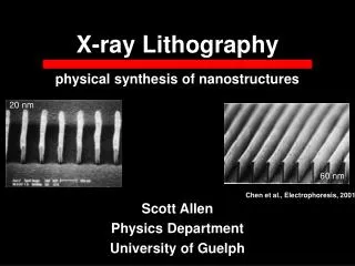
Micro - contact printing (μCP) 100mm stamp 20m
Micro - contact printing (μCP) Test structures in Au, smallest dimension 400nm
Micro - contact printing (μCP), with roller Printing on a planar surface with a planar stamp. Printing on a planar surface with a rolling stamp Printing on a non-planar surface with a planar stamp Xia & Whitesides, Angew. Chem. Int. Ed. 1998, 37, 550-575. A. Kumar & G. Whitesides, Applied Physics Lett. 1993
Self - assembling, classical –SH and Au bonding • Definition: spontaneous organization of molecules (objects) into stable, well-defined structures by non-covalent forces. • Driving force: thermodynamic equilibrium. • Final structure: determined by the subunits. • Biological 3D self assembly: folding of proteins, formation of DNA helix… Self assembled monolayer (SAM) Chemi-sorption and self-organization of long-chain organic molecules on flat substrates. Alkanethiolates CH3(CH2)nS-Au(111) -SH also bond to Ag, but Ag surface not as stable as Au. Laibinis,Whitesides, et al. JACS 1991, 113, 152
Applying alkanethiols on stamp to form SAM • These monolayers allow control over wettability, adhesion, chemical reactivity, electrical conduction, and mass transport to underlying metal • Linear alkanethiols with various molecular weights • 158 g/mol (dodecanethiol, DDT) • 258 g/mol (hexadecanethiol, HDT) • 314 g/mol (eicosanethiol, ECT) in ethanol Xia, Y.; Whitesides, G. M. Angew. Chem., Int. Ed. 1998, 37, 550. Michel, B.; Bernard, A., et al. IBM J. Res. & Dev. 2001, 45, 697.
Popular “ink” molecules Substrate Molecules
Patterning of palladium catalyst for electroless Cu plating Ink: bis-(stearonitrile)palladium-dichloride SEM images of Cu deposited onto catalytic Pd lines
Patterning of organic single crystals a. Procedure used to grow organic single crystals on substrates that have been patterned by microcontact printing. To grow the patterned single crystals, the patterned substrate is placed in a glass tube with the organic source material, vacuum-sealed (0.38 mmHg), and placed in a temperature gradient furnace tube. b–d, Patterned single-crystal arrays of different organic semiconductor materials. The dotted square in each image indicates the size and location of one of the OTS-stamped domains, while the molecular structure of the organic material used is shown next to the image of its single-crystal array. The above three materials are all hydrophobic and they binds/sticks to OTS (optical micrograph) Nature 444, 913-917 (14 December 2006) http://www.nature.com/nature/journal/v444/n7121/pdf/nature05427.pdf OTS: octadecyltrichlorosilane
Conformal micro-contact printing on rough surfaces Conformal contact between a soft stamp and a hard substrate. Dependence of maximal roughness amplitude for spontaneous formation of conformal contact on the roughness wavelength () for a stamp with Young's modulus of 2.5 MPa and work of adhesion of 0.1J/m² (Sylgard 184, solid line) and for a stamp with modulus of 9 MPa and work of adhesion of 0.03J/m² (dotted line). Larger allows for higher roughness.
Micro-contact printing on curved substrates PDMS is soft, it can roll onto curves Whitesides, “Fabrication of submicrometer features on curved substrates by microcontact printing”, Science, 269, 664 (1995); Rogers and Whitesides, “Microcontact Printing and Electroplating on Curved Substrates: Production of Free-Standing Three-Dimensional Metallic Microstructures”, Adv. Mater. 9, 475 (1997).
Pattern transfer into Si(100) by anisotropic etching Au Si KOH anisotropic etching of Si is the most popular pattern transfer technique when the etching mask is too thin for liftoff or direct etch. But it is limited to Si along certain crystalline directions.
Microcontact printing of proteins BSA: bovine serum albumin, bovine albumin
Microcontact printing of proteins Fluorescent image (anti-Goat IgG – Alexa 488 and 594)
Micro-contact printing of DNA Scheme of DNA printing. The surface of PDMS was modified such that it exposed positive charges on its surface. The stamp was incubated with target DNA molecules in a solution of low pH. The stamp was then rinsed, blown dry, and printed to deliver the DNA to the target surface. Fluorescence images of patterned FITC-labeled DNA on a glass surface after printing. AFM images revealing the printed DNA molecules deposited as patterns on mica substrates. AFM images (tapping mode in air) of stamped 1-μm lines of oligonucleotides (left, 20-bp oligos; right, 500-bp PCR fragments). S.A. Lange, V. Benes, D.P. Kern, J.K.H. Horber, A. Bernard, Anal. Chem. 2004, 76, 1641.
“Soft” lithography Soft lithography and PDMS. Micro-contact printing. Replica molding. Micro-molding in capillary. Micro-transfer molding/printing. Solvent assisted microcontact molding.
Replica molding (REM) It is similar to UV-curable nanoimprint lithography PU = polyurethane Xia & Whitesides et al, Advanced Materials, 1997, 9, 147
Replica molding (REM) The patterning process has high fidelity, with little feature size loss.
Using mold elasticity Molding on curved surface Creating curved surface Mechanical compression for feature size reduction Y. Xia et al., Science 1996
“Soft” lithography Soft lithography and PDMS. Micro-contact printing. Replica molding. Micro-molding in capillary. Micro-transfer molding/printing. Solvent assisted microcontact molding.
Micro-molding in capillary (MIMIC) Uses capillary forces to fill the gaps between substrate and PDMS master. The PDMS master is pressed tightly on a planar substrate. Elastic PDMS seals off walls and creates capillary channels. A drop of liquid prepolymer is placed at the ends of these channels and fills them automatically due to capillary force. PDMS can absorb the solvent, which creates a partial vacuum inside the PDMS cavity and helps to draw in liquid polymer. Cure and peel of the PDMS master. Liquid pre-polymer Nano-molding in capillaries is possible Line-width: 100nm
Micro-molding in capillary (MIMIC) a: PU (polyurethane) on Si b: polyaniline c: ZrO2 d: polystryene colloids e+f: free standing PU Kim & Whitesides et al, Nature, 1995, 376, 581 Xia, Y.; Whitesides, G. M. Ann. Rev. Mater. Sci 1998, 28, 153.
“Soft” lithography Soft lithography and PDMS. Micro-contact printing. Replica molding. Micro-molding in capillary. Micro-transfer molding/printing. Solvent assisted microcontact molding.
Micro - transfer molding (μTM) Pre-polymer PDMS Substrate • Apply the liquid prepolymer • Planarize the prepolymer • Place the master on a planar substrate • UV exposure or heating solidifies the prepolymer that sticks to the substrate TM fabrication of a). one-layer microstructures; b). three-layer polymer microstructures.
Micro - transfer molding (μTM) Microstructures fabricated using TM. An SEM image of a fractured sample showing a pattern of isolated stars of UV-cured polyurethane (NOA 73) on Ag. An array of parallel lines of spin-on glass on Si with an aspect ratio (height/width) of 8. A two-layer structure: isolated micro-cylinders (1.5m in diameter) on 5m-wide lines, supported on a glass cover slide. A two-layer structure: a continuous web over a layer of 5m-wide lines, supported on a glass cover slide. A three-layer structure on a glass cover slide. The layers of 4 m-wide lines are oriented at 60o from each other. Structures in c-e were made of heat-cured epoxy (F109CLR). Zhao & Whitesides et al, Advanced Materials, 1996, 8, 837.
Metal transfer assisted nanolithography SEM image of the transferred metal grating onto PMMA layer with period of 700nm on SiO2 substrate. Period 220nm on PET substrate. After O2 RIE of b. After metallization and lift-off process of c. Guo, “Metal transfer assisted nanolithography on rigid and flexible substrates”, JVST B, 2008
Metal transfer assisted nanolithography: line-width reduction SEM image of the metal grating on PET substrate after line-width reduction. The inset is a zoom-in view showing that the line-width was reduced to 50nm. Schematic of shadow (angle) evaporation of metals to reduce pattern line-width. The line-width is reduced by the thickness of the metal on the PDMS grating sidewall.
“Soft” lithography Soft lithography and PDMS. Micro-contact printing. Replica molding. Micro-molding in capillary. Micro-transfer molding/printing. Solvent assisted microcontact molding.
Solvent assisted microcontact molding (SAMIM) (solvent assisted imprinting) Substrates Silicon Glass Flexible transparency Polymer SU-8 (1μm) Shipley 1805 Photoresist (500nm) 3% PMMA (70nm) Solvent SU-8 (ethanol) Shipley 1805 photoresist (ethanol) 3% PMMA (acetone) The molded polymer structure becomes solidified in a few minutes after evaporation of solvent, while the stamp is still in conformable contact with the substrate. Uses a solvent to wet the PDMS stamp and soften the structure polymer. Dissipate and evaporate the solvent through PDMS. (PDMS stamp can absorb the solvent because of the solvent permeability of PDMS.) Kim & Whitesides et al, Advanced Materials, 1997, 9,651.
SAMIM of SU-8 in ethanol 2m diameter SU-8
SAMIM of PMMA in acetone Au structure fabrication
SAMIM of PMMA in acetone Hole array in PMMA Au dot array after liftoff Dot diameter 160nm.
Injection molding Very old technology, capable of micro-resolution, much higher throughput than hot embossing, good for microfluidic channel fabrication using thermoplastic polymers. (Thermoplastic polymer is better than PDMS for its “clean non-sticky” channel wall) Mold material: metal Required pressure: 500-200bars • The mold is heated to the softening temperature of the polymer to prevent the injected polymer material from hardening too early. • The reciprocating screw shears, melts, and pumps the polymer into the accumulation zones. • After cooling, the melt solidifies, and can be taken out from the mold.
Soft lithography: advantages and disadvantages • Advantages: • Convenient and low cost • Based on self assembly • Rapid prototyping • Deformation of PDMS provides route to complex patterns • No optical diffraction limit • Non-planar or curved surfaces • Generation of 3D -structures • Control over surface chemistry • A broad range of materials • Applicable to manufacturing • Patterning over large areas • Disadvantages: • Distortion of patterns • Poor registration/alignment • Compatibility with IC processes • Defects and their densities • μCP can only be applied to a number of surfaces • MIMIC is a relatively slow process • μTM and replica molding may leave thin polymer films between the relief structures
PDMS elastomer for mold making (coat mold release agent) University of Washington