Download
1 / 11
120 likes | 488 Vues
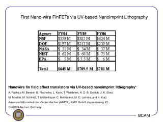
First Nano-wire FinFETs via UV-based Nanoimprint Lithography. Nanowire fin field effect transistors via UV-based nanoimprint lithography * A. Fuchs,a M. Bender, U. Plachetka, L. Kock, T. Wahlbrink, H. D. B. Gottlob, J. K. Efavi,

E N D
First Nano-wire FinFETs via UV-based Nanoimprint Lithography Nanowire fin field effect transistors via UV-based nanoimprint lithography* A. Fuchs,aM. Bender, U. Plachetka, L. Kock, T. Wahlbrink, H. D. B. Gottlob, J. K. Efavi, M. Moeller, M. Schmidt, T. Mollenhauer, C. Moormann, M. C. Lemme, and H. Kurz Advanced Microelectronic Center Aachen (AMICA), AMO GmbH, Huyskensweg 25, D-52074 Aachen, Germany
Outline • Nanoimprint • UV-Nanoimprint • FinFETs • Fabrication of FinFETs • Performance of FinFETs fabricated
Introduction to Nanoimprint Nanoimprint lithography (NIL) Conventional NIL processes, coined as stamp and step processes require thermal cycles between 140°C and 180°C and high pressures during the hot embossing procedure. Thermal and mechanical loads involved in these processes represent a nearly prohibitive burden for fast and high precision alignment. The mechanical masses to be moved in high throughput equipment require a large degree of complex mechanical handling.
Background on UV-Nanoimprint UV based nanoimprint lithography (UV-NIL) The low pressure (<1bar) as well as the absence of any thermalcycles appears very attractive for high precision printing down to 10 nm and relaxes the technical requirements for placement accuracy and pattern fidelity to a large extent.
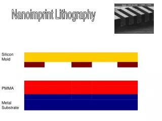
Wafer level UV-Nanoimprint • Step & Repeat UV Nanoimprint • A resist is spin coated on the substrate. • For highest resolution and minimum distortion a rigid fused silica template is used to imprint features die by die. The template is pressed into a thin layer of imprint resist via uniform pressure of a few hundred millibar. • After alignment of substrate and template in contact UV light is used to harden the resist. • After detachment the template is moved to the next position on the wafer and the process is repeated until the wafer is completely patterned.
Process flow of FinFETs via UV-Nanoimprint 5 mm thick 1in mold used with 150nm deep features. 1. Pattern the S/D and channel structure a. Imprint process at reduced ambient pressure 20 mbars and imprint pressure of 300mbars. b. UV curing resist---mold detached---RIE etching 2. CVD polysilicon for gate (heavily doped) 3. Pattern the gate 4. S/D implantation (As=2 x 10E20 ions/cm^2)
Performance result of FinFETs Transistor output characteristics exhibits linear and saturation regions!!! Typical field effect transistor behavior is clearly observed!!! Wait…….
Conclusion • Promising approach. • Yield?? Questions???