Chapter 10 HCS12 Serial Peripheral Interface
Chapter 10 HCS12 Serial Peripheral Interface. What is Serial Peripheral Interface (SPI)?. SPI is a synchronous serial protocol proposed by Motorola to be used as standard for interfacing peripheral chips to a microcontroller. Devices are classified into the master or slaves.

Chapter 10 HCS12 Serial Peripheral Interface
E N D
Presentation Transcript
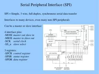
What is Serial Peripheral Interface (SPI)? • SPI is a synchronous serial protocol proposed by Motorola to be used as standard for interfacing peripheral chips to a microcontroller. • Devices are classified into the master or slaves. • The SPI protocol uses four wires to carry out the task of data communication: • MOSI: master out slave in • MISO: master in slave out • SCK: serial clock • SS: slave select • An SPI data transfer is initiated by the master device. A master is responsible for generating the SCK signal to synchronize the data transfer. • The SPI protocol is mainly used to interface with shift registers, LED/LCD drivers, phase locked loop chips, memory components with SPI interface, or A/D or D/A converter chips.
The HCS12 SPI Modules • An HCS12 device may have from one to three SPI modules. • The MC9S12DP256 has three SPI modules: SPI0, SPI1, and SPI2. • By default, the SPI0 share the use of the upper 4 Port S pins: • PS7 SS0 (can be rerouted to PM3) • PS6 SCK0 (can be rerouted to PM5) • PS5 MOSI0 (can be rerouted to PM4) • PS4 MISO0 (can be rerouted to PM2) • By default, the SPI1 shares the use of the lower 4 Port P pins: • PP3 SS1 (can be rerouted to PH3) • PP2 SCK1 (can be rerouted to PH2) • PP1 MOSI1 (can be rerouted to PH1) • PP0 MISO1 (can be rerouted to PH0) • By default, the SPI2 shares the use of the upper 4 Port P pins: • PP6 SS2 (can be rerouted to PH7) • PP7 SCK2 (can be rerouted to PH6) • PP5 MOSI2 (can be rerouted to PH5) • PP4 MISO2 (can be rerouted to PH4) • It is important to make sure that there is no conflict in the use of signal pins when making rerouting decision.
SPI Related Registers (1 of 6) • The operating parameters of each SPI module are controlled via two control registers: • SPIxCR1: (x = 0, 1, or 2) • SPIxCR2 • The baud rate of SPI transfer is controlled by the SPIxBR register. • The operation status of the SPI operation is recorded in the SPIxSR register. • The contents of the SPIxCR1, SPIxCR2, SPIxBR, and SPIxSR registers are illustrated in Figure 10.1 to 10.4, respectively. • The SS pin may be disconnected from SPI by clearing the SSOE bit in the SPIxCR1 register. After that, it can be used as a general I/O pin. • If the SSOE bit in the SPIxCR1 register is set to 1, then the SS signal will be asserted to enable the slave device whenever a new SPI transfer is started. • The equation for setting the SPI baud rate is given in Figure 10.3.
SPI Related Registers (6 of 6) • Example 10.1 Give a value to be loaded to the SPIxBR register to set the baud rate to 2 MHz for a 24 MHz bus clock. • Solution: 24 MHz 2 MHz = 12. One possibility is to set SPPR2-SPPR0 and SPR2-SPR0 to 010 and 001, respectively. The value to be loaded into the SPIxBR register is $21. • Example 10.2 What is the highest possible baud rate for the SPI with 24 MHz bus clock? • Solution: The highest SPI baud rate occurs when both the SPPR2-SPPR0 and SPR2-SPR0 are 000. In this case the baud rate is 24 MH 2 = 12 MHz.
SPI Transmission Format (1 of 3) • The data bits can be shifted on the rising or the falling edge of the SCK clock. • Since the SCK can be idle high or idle low, there are four possible combinations as shown in Figure 10.5 and 10.6. • To shift data bits on the rising edge, set CPOL-CPHA to 00 or 11. • To shift data bits on the falling edge, set CPOL-CPHA to 01 or 10. • Data byte can be shifted in and out most significant bit first or least significant bit first.
Bidirectional Mode (MOMI or SISO) • A mode that uses only one data pin to shift data in and out. • This mode is provided to deal with peripheral devices with only one data pin. • Either the MOSI pin or the MISO pin can be used as the bidirectional pin. • When the SPI is configured to the master mode (MSTR bit = 1), the MOSI pin is used in data transmission and becomes the MOMI pin. • When the SPI is configured to the slave mode (MSTR bit = 0), the MISO pin is used in data transmission and becomes the SISO pin. • The direction of each serial pin depends on the BIDIROE bit of the SPIxCR2 register. • The pin configuration for MOSI and MISO are illustrated in Figure 10.7. • If one wants to read data from the peripheral device, clear the BIDIROE bit to 0. • If one wants to output data to the peripheral device, set the BIDIROE bit to 1. • The use of the this mode is illustrated in exercise problem 10.8.
Mode Fault Error • If the SSx signal goes low while the SPIx is configured as a master, it indicates a system error where more than one master may be trying to drive the MOSIx and SCKx pins simultaneously. • The MODF bit in the SPIxSR register will be set to 1 when mode fault condition occurs. • When mode fault occurs, the MSTR bit will be cleared to 0 and the output enable for the MOSIx and SCKx pins will be deasserted.
SPI Circuit Connection • In an SPI system, one device is configured as a master. Other devices are configured as slaves. • The circuit connection for a single-slave system is shown in Figure 10.8. • A multi-slave system may have two different connection methods as illustrated in Figure 10.9 and 10.10. • In Figure 10.9, the master can exchange data with each individual slave without affecting other slaves. • In Figure 10.10, all the slaves are configured into a larger ring. A data transmission with certain slaves will go through other slaves.
Example 10.3 Configure the SPI0 to operate with the following setting assuming that E • clock is 24 MHz: • 6 MHz baud rate • Enable SPI0 to master mode • SCK0 pin idle low with data shifted on the rising edge of SCK • Transfer data most significant bit first and disable interrupt • Disable SS0 function • Stop SPI in Wait mode • Normal SPI operation (not bidirectional mode)
Solution: fE / baud rate = 24 MHz/6 MHz = 4. We need to set SPPR2-SPPR0 and SPR2-SPR0 to 001 and 000, respectively. Write the value $10 into the SPI0BR register. • The following instruction sequence will configure the SPI0 as desired: movb #$10,SPI0BR ; set baud rate to 6 MHz movb #$50,SPI0CR1 ; disable interrupt, enable SPI, SCK idle low, data ; latchedon rising edge, data transferred msb first movb #$02,SPI0CR2 ; disable bidirectional mode, stop SPI in wait mode movb #0,WOMS ; enable Port S pull-up
SPI Utility Functions • The following operations are common in many applications and should be made into library functions to be called by many SPI applications: • Send a character to SPI putcspix (x = 0, 1, or 2) • Send a string to SPI putsspix (x = 0, 1, or 2) • Read a character from SPI getcspix (x = 0, 1, or 2) • Read a string from SPI getsspix (x = 0, 1, or 2)
Function putcSPI0 putcspi0 brclr SPI0SR,SPTEF,* ; wait until write operation is permissible staa SPI0DR ; output the character to SPI0 brclr SPI0SR,SPIF,* ; wait until the byte is shifted out ldaa SPI0DR ; clear the SPIF flag rts void putcspi0 (char cx) { char temp; while(!(SPI0SR & SPTEF)); /* wait until write is permissible */ SPI0DR = cx; /* output the byte to the SPI */ while(!(SPI0SR & SPIF)); /* wait until write operation is complete */ temp = SPI0DR; /* clear the SPIF flag */ }
Function putsSPI0 ; the string to be output is pointed to by X putsspi0 ldaa 1,x+ ; get one byte to be output to SPI port beq doneps0 ; reach the end of the string? jsr putcspi0 ; call subroutine to output the byte bra putsspi0 ; continue to output doneps0 rts void putsspi0(char *ptr) { while(*ptr) { /* continue until all characters have been output */ putcspi0(*ptr); ptr++; } }
Function getcSPI0 ; This function reads a character from SPI0 and returns it in accumulator A getcspi0 brclr SPI0SR,SPTEF,* ; wait until write operation is permissible staa SPI0DR ; trigger eight clock pulses for SPI transfer brclr SPI0SR,SPIF,* ; wait until a byte has been shifted in ldaa SPI0DR ; return the byte in A and clear the SPIF flag rts char getcspi0(void) { while(!(SPI0SR & SPTEF)); /* wait until write is permissible */ SPI0DR = 0x00; /* trigger 8 SCK pulses to shift in data */ while(!(SPI0SR & SPIF)); /* wait until a byte has been shifted in */ return SPI0DR; /* return the character */ }
Function getsSPI0 ; This function reads a string from the SPI and store it in a buffer pointed to by X ; The number of bytes to be read in passed in accumulator B getsspi0 tstb ; check the byte count beq donegs0 ; return when byte count is zero jsr getcspi0 ; call subroutine to read a byte staa 1,x+ ; save the returned byte in the buffer decb ; decrement the byte count bra getsspi0 donegs0 clr 0,x ; terminate the string with a NULL character rts void getsspi0(char *ptr, char count) { while(count) { /* continue while byte count is nonzero */ *ptr++ = getcspi0(); /* get a byte and save it in buffer */ count--; } *ptr = 0; /* terminate the string with a NULL */ }
The HC595 Shift Register • The HC595 consists of an 8-bit shift register and a D-type latch with three-state parallel output. • The shift register provides parallel data to the latch. • The maximum data shift rate is 100 MHz (Philips part).
Signal Pins of the HC595 • DS: serial data input • SC: shift clock. A low-to-high transition on this pin causes the data at the serial input pin to be shifted into the 8-bit shift register. • Reset: A low on this pin resets the shift register portion of this device. • LC: latch clock. A low-to-high transition on this pin loads the contents of the shift register into the output latch. • OE: output enable. A low on this pin allows the data from the latches to be presented at the outputs. • QA to QH: tri-state latch output • SQH: the output of the eight stage of the shift register
Applications of the HC595 (1 of 2) • The HC595 is often used to add parallel ports to the microcontroller. • Both the connection methods shown in Figure 10.9 and 10.10 can be used to add parallel ports to the MCU.
Applications of the HC595 (2 of 2) • Example 10.5 Describe how to use two 74HC595s to drive eight common cathode seven-segment displays assuming that the E clock frequency of the HCS12 is 24 MHz. • Solution: Use the circuit in figure 10.12 to connect two 74HC595s to the HCS12.
Program to display 87654321 on display #7 to #0 #include “c:\miniide\hcs12.inc" org $1000 icnt ds.b 1 ; loop count org $1500 lds #$1500 ; set up stack pointer bset DDRK,$80 ; configure the PK7 pin for output jsr openspi0 ; configure SPI0 forever ldx #dispTab ; use X as a pointer to the table movb #8,icnt ; set loop count to 8 loop ldaa 1,x+ ; send the digit select byte to the 74HC595 jsr putcspi0 ; " ldaa 1,x+ ; send segment pattern to 74HC595 jsr putcspi0 ; " bclr PTK,BIT7 ; transfer data from shift register to output bset PTK,BIT7 ; latch ldy #1 ; display the digit for one ms jsr delayby1ms ; " dec icnt ; bne loop ; if not reach digit 1, then next bra forever ; start from the start of the table
openspi0 movb #0,SPI0BR ; set baud rate to 12 MHz movb #$50,SPI0CR1 ; disable interrupt, enable SPI, SCK idle low, ; latch data on rising edge, transfer data msb first movb #$02,SPI0CR2 ; disable bidirectional mode, stop SPI in wait mode movb #0,WOMS ; enable Port S pull-up rts #include "c:\miniide\delay.asm" #include "c:\miniide\spi0util.asm" ; ******************************************************************** ; Each digit consists of two bytes of data. The first byte is ; digit select, the second byte is the digit pattern. ; ******************************************************************** dispTab dc.b $80,$7F,$40,$70,$20,$5F,$10,$5B dc.b $08,$33,$04,$79,$02,$6D,$01,$30 end
#include “c:\egnu091\include\hcs12.h” #include “c:\egnu091\include\spi0util.c” #include “c:\egnu091\include\delay.c” void openspi0(void); void main (void) { unsigned char disp_tab[8][2] = {{0x80,0x7F},{0x40,0x70},{0x20,0x5F},{0x10,0x5B}, {0x08,0x33},{0x04,0x79},{0x02,0x6D},{0x01,0x30}}; char i; openspi0(); /* configure the SPI0 module */ DDRK |= BIT7; /* configure pin PK7 as output */ while(1) { for (i = 0; i < 8; i++) { putcspi0(disp_tab[i][0]); /* send out digit select value */ putcspi0(disp_tab[i][1]); /* send out segment pattern */ PTK &= ~BIT7; /* transfer values to latches of 74HC595s */ PTK |= BIT7; /* " */ delayby1ms(1); /* display a digit for 1 ms */ } } }
The TC72 Digital Thermometer • 10-bit resolution and SPI interface • Pin assignment and block diagram shown in Figure 10.13. • Capable of reading temperature from -55oC to 125oC. • Can be used in continuous temperature conversion or one-shot conversion mode. • Has internal clock generator to control the automatic temperature conversion sequence
Temperature Data Format • Temperature is represented by a 10-bit two’s complement word with a resolution of 0.25oC per least significant bit. • The converter is scaled from -128oC to +127oC with 0oC represented as 0x0000. • The temperature value is stored in two 8-bit registers. • Whenever the most significant bit is 1, the temperature is negative. • A sample of temperature reading is shown.
TC72’s Serial Interface • The CE input to the TC72 must be asserted (high) to enable SPI transfer. • Data can be shifted on the rising edge or the falling edge depending on the idle polarity of the SCK source. • Data transfer to and from the TC72 consists of one address byte followed by one or multiple data (2 to 4) bytes. • The TC72 registers and their addresses are shown in Table 10.4. • The most significant bit of the address byte determines whether a read (A7 = 0) or a write (A7 = 1) operation will occur. • A multiple byte read operation will start from high address toward lower addresses. • The user can send in the temperature result high byte address and read the temperature result high byte, low byte, and the control registers.
Procedure for Reading Temperature (1 of 2) • Step 1 • Pull the CE pin high to enable SPI transfer. • Step 2 • Send the temperature result high byte read address (0x02) to the TC72. Wait until the SPI transfer is complete. • Step 3 • Read the temperature result high byte. The user needs to write a dummy byte into the SPI data register to trigger eight clock pulses. • Step 4 • Read the temperature result low byte. Again, the user needs to write a dummy byte into the SPI data register to trigger eight clock pulses. • Step 5 • Pull CE pin to low so that a new transfer can be started. • Single-byte read and multiple-byte read timing diagrams are shown in Figures 10.15b and 10.15c.
Control Register • The control register is used to select the shutdown, continuous, or one-shot conversion operating mode. • The temperature conversion mode selection logic is shown in Table 10.5. • At power up, the SHDN bit is 1. Thus the TC72 is in the shutdown mode. • If the SHDN bit is 0, the TC72 will perform a temperature conversion approximately every 150 ms. • A temperature conversion will be initiated by a write operation into the control register to select the continuous mode or one-shot mode. • A typical circuit connection between the TC72 and the HCS12 is shown in Figure 10.16.
Example 10.6 Write a C program to read the temperature every 200 ms. Convert the temperature to a string so that it can be displayed in an appropriate output device. A pointer to hold the string will be passed to this function. The bus clock is 24 MHz.
#include “c:\egnu091\include\hcs12.h” #include “c:\egnu091\include\spi0util.c” #include “c:\egnu091\include\delay.c” #include “c:\egnu091\include\convert.c” void read_temp (char *ptr); void openspi0(void); char buf[10]; void main (void) { DDRM |= BIT1; /* configure the PM1 pin for output */ openspi0(); /* configure SPI0 module */ read_temp(&buf[0]); } void openspi0(void) { SPI0BR = 0x10; /* set baud rate to 6 MHz */ SPI0CR1 = 0x50; /* enable SPI0 to master mode, select rising edge to shift data in and out */ SPI0CR2 = 0x02; /* select normal mode and stop SPI in wait mode */ WOMS = 0x00; /* enable Port S pull-up */ }
void read_temp (char *ptr) { char hi_byte, lo_byte, temp, *bptr; unsigned int result; bptr = ptr; PTM |= BIT1; /* enable TC72 data transfer */ putcspi0(0x80); /* send out TC72 control register write address */ putcspi0(0x11); /* perform one shot conversion */ PTM &= ~BIT1; /* disable TC72 data transfer */ delayby100ms(2); /* wait until temperature conversion is complete */ PTM |= BIT1; /* enable TC72 data transfer */ putcspi0(0x02); /* send MSB temperature read address */ hi_byte = getcspi0(); /* read the temperature high byte */ lo_byte = getcspi0(); /* save temperature low byte and clear SPIF */ PTM &= ~BIT1; /* disable TC72 data transfer */ lo_byte &= 0xC0; /* make sure the lower 6 bits are 0s */ result = (int) hi_byte * 256 + (int) lo_byte; if (hi_byte & 0x80) { /* temperature is negative */ result = ~result + 1; /* take the two' complement of result */ result >>= 6;
temp = result & 0x0003; /* place the lowest two bits in temp */ result >>= 2; /* get rid of fractional part */ *ptr++ = 0x2D; /* store the minus sign */ int2alpha(result, ptr); } else { /* temperature is positive */ result >>= 6; temp = result & 0x0003; /* save fractional part */ result >>= 2; /* get rid of fractional part */ int2alpha(result, ptr); /* convert to ASCII string */ } while(*bptr){ /* search the end of the string */ bptr++; }; switch (temp){ /* add fractional digits to the temperature */ case 0: break; case 1: /* fractional part is .25 */ *bptr++ = 0x2E; /* add decimal point */ *bptr++ = 0x32; *bptr++ = 0x35; *bptr = '\0'; break;
case 2: /* fractional part is .5 */ *bptr++ = 0x2E; /* add decimal point */ *bptr++ = 0x35; *bptr = '\0'; break; case 3: /* fractional part is .75 */ *bptr++ = 0x2E; /* add decimal point */ *bptr++ = 0x37; *bptr++ = 0x35; *bptr = '\0'; break; default: break; } }
The D/A Converter TLV5616 • The TLV5616 is a 12-bit voltage output digital-to-analog converter (DAC) with SPI interface. • The TLV5616 has an output settling time of 3 ms in fast mode and 9 ms in slow mode. • A D/A conversion is started by writing a 16-bit serial string that contains 4 control bits and 12 data bits to the TLV5616. • TLV5616 can operate from 2.7V to 5.5V.
TLV5616 Signal Pins • AGND: analog ground • CS: chip select (active low) • DIN: serial data input • FS: frame sync • OUT: DAC analog output • REFIN: reference analog input voltage • SCLK: serial clock input • VDD: positive power supply
Date Format - A 16-bit frame with 4 control bits and 12 data bits.
TLV5616 Output Voltage • The output voltage is given by the following expression: • VOUT = 2 REF code 2n • The reference voltage input cannot be higher than VDD/2.
Data Shifting Timing • The FS pulse must be generated before data shifting can start. • The highest data shift rate is 20 MHz.
CS and FS Trigger Sequence • Pull FS to high. • Pull CS to low. • Pull FS to low. • Send out control and data bits using the SPI transfer. • Wait until all 16 bits have been shifted out; pull FS to high. • Pull CS to high.
Example 10.9 Write a program to generate a waveform that is a repetition of the • waveform shown in Figure 10.21 using the circuit shown in Figure 10.20. • The values to be sent to the TLV5616 to generate 0V, 1V, 2V, and 3V outputs are: • val(0) = 0 • val(1) = 212/4 = 1024 • val(2) = 2 212/4 =2048 • val(3) = 3 212/4 = 3072 • The 16-bit values (in fast mode) to be written to the TLV5616 for this four voltages are • as follows: • code (0) = $4000 • code (1) = $4400 • code (2) = $4800 • code (3) = $4C00