Download
1 / 25
690 likes | 1.58k Vues
DIGITAL SIGNAL PROCESSOR. FIXED POINT/FLOATING POINT DSP HARVARD/VON NEUMANN ARCHITECTURE RISC/CISC ARCHITECTURE PIPELINING Architecture of TMS320C5X (Features-Description) Addressing Modes. Introduction. Application specific Processor.

E N D
DIGITAL SIGNAL PROCESSOR FIXED POINT/FLOATING POINT DSP HARVARD/VON NEUMANN ARCHITECTURE RISC/CISC ARCHITECTURE PIPELINING Architecture of TMS320C5X (Features-Description) Addressing Modes
Introduction • Application specific Processor. • Manufacturers: Texas Instruments, Analog Devices, Motorola • Two types: 16 bit fixed point and 32 bit floating point TMS320C5X: • Fifth generation • 16 bit fixed point processor • Instruction sets are upward compatible.
FIXED/FLOATING POINT PROCESSOR • 16 BIT FIXED POINT PROCESSOR: C1X, C2X, C2XX, C5X • 32 BIT FLOATING POINT PROCESSOR: C3X, C4X
RISC/CISC ARCHITECTURE CISC MULT 2:3, 5:2 RISC LOAD A, 2:3LOAD B, 5:2PROD A, BSTORE 2:3, A
What is CISC Complex Instruction Set Computer FEATURES: Instructions can operate directly on memory Small number of general purpose registers Instructions take multiple clocks to execute
What is RISC? Reduced Instruction Set Computer RISC is a CPU design that recognizes only a limited number of instructions Simple instructions Instructions are executed quickly
Features of RISC “Reduced” instruction set Executes a series of simple instruction instead of a complex instruction Instructions are executed within one clock cycle Incorporates a large number of general registers for arithmetic operations to avoid storing variables on a stack in memory Only the load and store instructions operate directly onto memory Pipelining = speed
PIPELINING Fetching the next instruction while the current instruction is decoding. The fundamental idea is to split the processing of a computer instruction into a series of independent steps. • FETCH • DECODE • MEMORY READ • EXECUTE
Instruction cycle: Fetching,decoding,memory read and execution of one instruction Machine Cycle: Memory or I/O operation requires a particular time period T-States: Each machine cycle consists of 3 to 6 clock cycles Program counter: Points the address of the next instruction to be fetched Stack Pointer: Points the return address.
ADDRESSING MODES Direct addressing Indirect addressing Immediate addressing Memory Mapped register addressing Circular addressing
Immediate addressing Load either a 16 bit constant or a constant of length 13, 9 0r 7. Accordingly it is referred to as long immediate or Short immediate addressing mode. Indicated by symbol # Eg ADD #56h ; ADD #4321h
DIRECT ADDRESSING Eg: ADD 98h,5
MEMORY MAPPED REGISTER ADDRESSING LAMM LMMR SAMM SMMR
CIRCULAR ADDRESSING Algorithms such as convolution, Correlation and FIR use Circular buffers in Memory
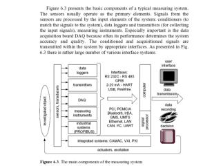
ARCHITECTURE - DESCRIPTIONS • Running at 40MHz • Execution time of single instruction is 50nsec • On-Chip memory include 10k words of RAM and 2K words of the ROM. • The Function block is divided into 4 sub blocks. • BUS STRUCTURE • CPU • ONCHIP MEMORY • ONCHIP PERIPHERALS
BUS STRUCTURE • PROGRAM BUS interconnects CPU and Program memory • PROGRAM ADDRESS BUS Provides address to program memory space for read and write. • DATA BUS Interconnects various elements in CPU and data memory • DATA ADDRESS BUS Provides address to access the data memory space
CPU • Central Arithmetic Logic Unit MAC [16x16 parallel multiplier, 32 bit Accumulator, 32- bit ACC Buffer, Product register, additional shifter] • Parallel Logic Unit – logical operation • Auxiliary register arithmetic Unit – [AR0 – AR7, ARP, indirect addressing] • Memory Mapped registers - [SFR, page 0 (00-5F)] • Program Controller • Program counter • Status and Control register – 4 status and control registers. • Hardware stack - 8 levels deep, 16 bit wide • Program memory Address generation logic - address gen by program counter • Instruction register – hold the opcode.
ONCHIP MEMORY • Memory address range: 224kwordsx16bits • Memory space is divided into 4 memory segments: 64k words - program memory space 64k words - local data memory space 64k words - input/ output ports 32 k words – Global data memory space On chip memory includes: • PROM - MP/MC • Data/Program single access RAM - [configured as program/data or both] • Data/Program dual access RAM [B0 – program /Data]
ON-CHIP PERIPHERALS • Clock generator.-internal oscillator &PLL • Hardware timer.-generate CPU interrupts • Software programmable wait state generator. -Can extend external bus cycles up to 7 m/c cycles • General purpose I/O pins. - Branch control i/p(BIO) to monitor pheripheral device status -XF pin signals to external devices via S/w • Parallel I/O ports.-64 parallel i/o ports • Serial port interface. • Buffered serial port. • TDM serial port. • Host port interface.- to interface host device to c5x • User unmaskable interrupts.- interrupt due to external devices