Nanocharacterization of Materials with Aberration-Corrected Analytical Electron Microscope
20 likes | 111 Vues
Acquisition of an aberration-corrected analytical electron microscope enhances imaging and spectroscopic capabilities for nanomaterial characterization. Research focuses on microstructure analysis and elemental mapping with high precision.

Nanocharacterization of Materials with Aberration-Corrected Analytical Electron Microscope
E N D
Presentation Transcript
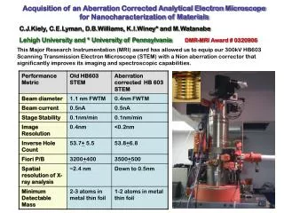
Acquisition of an Aberration Corrected Analytical Electron Microscope for Nanocharacterization of Materials C.J.Kiely, C.E.Lyman, D.B.Williams, K.I.Winey* and M.Watanabe Lehigh University and * University of PennsylvaniaDMR-MRI Award # 0320906 This Major Research Instrumentation (MRI) award has allowed us to equip our 300kV HB603 Scanning Transmission Electron Microscope (STEM) with a Nion aberration corrector that significantly improves its imaging and spectroscopic capabilities.
Zr Pd Au 20 0 0.5 0 (atoms) 2nm 50nm 10nm (wt%) Zr segregation at a g- g’ grain boundary in a Ni- based superalloy. Au-Pd catalyst particle on TiO2 showing Pd surface segregation. Irradiation induced Cu precipitates in a low alloy nuclear steel STEM-XEDS Spectrum Imaging: Some Applications Our previous world record for spatial resolution in X-Ray Energy Dispersive Spectroscopy(XEDS) has been beaten by a factor of 3. This has been achieved by adding a Nion aberration corrector to our HB 603 STEM which reduces the minimum attainable electron probe size from 1.5 to 0.5nm. Below are some recent materials science applications of this instrument. Microscopy. & Microanalysis (2006), in press. Journal of Materials Science (2006), 41, 4512 Science, (2006), 311, 362