Download
1 / 1
10 likes | 157 Vues
System Idea : It is a preliminary stage where we an idea is jotted down on paper or documented, a system is designed to meet the idea.

E N D
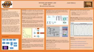
System Idea: It is a preliminary stage where we an idea is jotted down on paper or documented, a system is designed to meet the idea. Behavioral : A full system is designed using higher Level language like Verilog, Each system is divided into sub modules depending on the block which we designed in system design stage. RTL : Register Transfer Architectural HDL, a structural coding is done in this stage. Verilog code is optimized , hierarchical coding approach is used while designing. Synthesis : Synthesis has many definitions in itself, it can be best describe as forward progression of an idea towards Graphic Database System (GDS) which is the final stage of tape out. Synthesis has changed a lot these decades and it has evolve with the invention of new tools which deal with synthesis. Electronic Design tool (EDA) is the term with which most of the people are familiar. Gate Netlist: A final Gate netlist is generated after all the synthesis process, throughout the process our design keeps on optimizing and changes the requirement of basic standard cells which we had use at initial stage of our design. Layout: A complete cell boundary is identified and Pad for Analog circuits and Digital circuits are designed. We might also need some extra Pads for testing purpose Each pad has Electro static Discharge (ESD) circuit connected to it. • DRC and LVS: DRC stands for design rule check, where a design rule file is uploaded in cadence or synopsis which ever domain you are working. Below are some of the basic design rules which are checked before sending final file for fabrication. • FABRICATION OF CHIP: There are very few industries which do fabrication on larger scale. There are different types of fabrication process which are followed for example UMC might have a different fabrication process than IBM may have. • TSMC Fabrication Processes[3] • IBM Fabrication Processes[4] • ON Semiconductor Fabrication Processes[5] Materials used in a basic CMOS integrated circuit [1]: Si substrate – selectively doped in various regions SiO2 insulator Polycrystalline silicon – used for the gate electrode Metal contacts and wiring Fabrication schedule: Each fabrication process have a deadline for the Tape out design submission. We need to submit our design within time. For an instance an IBM fabrication process might have a schedule shown below. Reference [1] Prof. Dr. James Stine, VLSI System design ECEN 5263, Oklahoma state university [2] http://www.mosis.com/products/fab-processes [3] http://www.mosis.com/vendors/view/tsmc/processes [4] http://www.mosis.com/vendors/view/ibm [5] http://www.mosis.com/vendors/view/on-semiconductor/processes INTRODUCTION Application Specific Integrated Circuit(ASIC) is a personalized Integrated Circuit developed for an application. As the technology is developing rapidly, every field is having small area and low power design chips. Every ASIC design can have a processor, RAM, ROM, Register file, PLL, LDO and many more circuits which forms a (System On-Chip). A concept called Standard Cell library is used to design the chip and its layout. Standard cell library may contain all basic gates used for CMOS layout and schematic eg: NAND GATE, AND GATE, using those gates we can built a multiplexer, counter, register file etc. Thus we can design complete system’s schematic and layout. Software’s like Cadence Virtuoso and Synopsis are used for designing and making layout of complete system. Depending on the fabrication standards and limitations we need to create the standard cell library. Eg: IBM design standards and UMC design standards are different and a layout designed using IBM design standards won’t be used to fabricate the chip using UMC fabrication process. DEVICES AND DESIGN: ASIC - Aniket Kulkarni ECEN - 5843 Microelectronic Fabrication Design Flow and Abstraction: 2


![Progressive Enhancement & Mobile [Funka 2012]](https://cdn4.slideserve.com/7565260/progressive-enhancement-mobile-dt.jpg)