Divide-By-8 Counter Design for Arbitrary Waveform Generation
This document details a design for a divide-by-8 counter implemented to produce arbitrary waveforms. The counter utilizes state outputs Q2, Q1, and Q0 as inputs for a combinational circuit, generating defined waveform sequences based on pre-set state transitions. Detailed timing diagrams illustrate state changes along with input and output connections. Additionally, example equations for state transitions and output generation are provided to aid in understanding this complex logic design. The description adheres to standard digital design principles.

Divide-By-8 Counter Design for Arbitrary Waveform Generation
E N D
Presentation Transcript
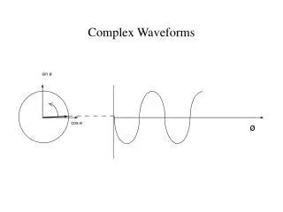
Arbitrary Waveforms Module M10.5 Section 7.2
State Q2 Q1 Q0 Q2.D Q1.D Q0.D D Q Q0.D Q0 CLK !Q s0 0 0 0 0 0 1 s1 0 0 1 0 1 0 s2 0 1 0 0 1 1 s3 0 1 1 1 0 0 s4 1 0 0 1 0 1 s5 1 0 1 1 1 0 s6 1 1 0 1 1 1 s7 1 1 1 0 0 0 D Q Q1.D Q1 CLK !Q D Q Q2.D Q2 CLK !Q Recall Divide-by-8 Counter Use Q2, Q1, Q0 as inputs to a combinational circuit to produce an arbitrary waveform.
Q1 Q0 1 1 00 01 11 10 Q2 0 1 1 1 1 1 0 0 0 1 0 1 1 1 0 0 0 1 0 1 Example (See Exercise 7.10) State Q2 Q1 Q0 Q2.D Q1.D Q0.D y s0 0 0 0 0 0 1 1 s1 0 0 1 0 1 0 1 s2 0 1 0 0 1 1 0 s3 0 1 1 1 0 0 0 s4 1 0 0 1 0 1 0 s5 1 0 1 1 1 0 1 s6 1 1 0 1 1 1 0 s7 1 1 1 0 0 0 1 y = !Q2 & !Q1 # Q2 & Q0
“ Inputs: PB PIN 10; “Clock “ Outputs: Q2..Q0 PIN 37,36,35 ISTYPE 'reg buffer'; " LED 6..8 Q = [Q2..Q0]; " 3-bit output vector Y PIN 44 ISTYPE ‘com’; “LED 1 EQUATIONS q0.d = !q0; q1.d = !q1 & q0 # q1 & !q0; q2.d = !q2 & q1 & q0 # q2 & !q1 # q2 & !q0; y = !q2 & !q1 # q2 & q0;
ORDER: clock,%2,q0,%2,q1,%2,q2,%2,y; VECTORS: C LLLH C HLLH C LHLL C HHLL C LLHL C HLHH C LHHL C HHHH C LLLH C HLLH C LHLL C HHLL C LLHL C HLHH C LHHL C HHHH CUPL Simulation File
CUPL Simulation Output File


![Concentration [arbitrary]](https://cdn2.slideserve.com/4860652/slide1-dt.jpg)