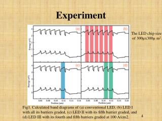
Experiment
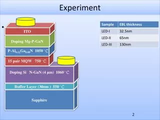
Experiment. Doping Mg-P- GaN. ITO. P-Al 0.12 Ga 0.88 N 1050 。 C. 15 pair MQW 750 。 C. Doping Si N- GaN (4 μ m) 1060 。 C. Buffer Layer (30nm ) 550 。 C. Sapphire. Result and Discussion.

Experiment
E N D
Presentation Transcript
Experiment DopingMg-P-GaN ITO P-Al0.12Ga0.88N1050。C 15 pair MQW750。C Doping Si N-GaN (4 μm)1060。C Buffer Layer (30nm )550。C Sapphire
Result and Discussion • Fig. 1. Measured ESD results as function of stress voltages and light output power as function of forward currents for the LEDs. The values shown in the right-hand vertical axis mean the total tested device numbers (100 devices) divided by the nonfailed device numbers for a given reverse stress voltage.
Fig. 2. Top-view SEM images of the LEDs: (a) LED-III and (b) LED-I. AFM images taken from the surface of p-AlGaN EBL without the LTG p-GaNtop layer corresponding to the LED-III and LED-I are also shown in the inset of Fig. 2(a) and (b), respectively.