Download
1 / 18
290 likes | 1.21k Vues
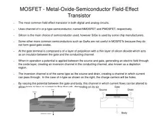
MOSFET - Metal-Oxide-Semiconductor Field-Effect Transistor. The most common field effect transistor in both digital and analog circuits. Uses channel of n or p-type semiconductor, named NMOSFET and PMOSFET, respectively.

E N D
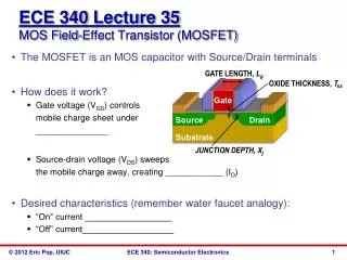
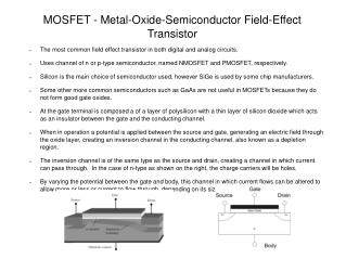
MOSFET - Metal-Oxide-Semiconductor Field-Effect Transistor • The most common field effect transistor in both digital and analog circuits. • Uses channel of n or p-type semiconductor, named NMOSFET and PMOSFET, respectively. • Silicon is the main choice of semiconductor used, however SiGe is used by some chip manufacturers. • Some other more common semiconductors such as GaAs are not useful in MOSFETs because they do not form good gate oxides. • At the gate terminal is composed a of a layer of polysilicon with a thin layer of silicon dioxide which acts as an insulator between the gate and the conducting channel. • When in operation a potential is applied between the source and gate, generating an electric field through the oxide layer, creating an inversion channel in the conducting channel, also known as a depletion region. • The inversion channel is of the same type as the source and drain, creating a channel in which current can pass through. In the case of n-type as shown on the right, the charge carriers will be holes. • By varying the potential between the gate and body, this channel in which current flows can be altered to allow more or less or current to flow through, depending on its size.
Bipolar Junction Transistor • First created in 1948 by Bell Telephone • Similar to the Mosfet • Reliable under severe conditions – dominant in automobiles • NPN and PNP • Digital logic circuits-Boolean
Downfalls of BJT- Large base current, ib, is needed to turn transistor on. • Electrons and holes contribute to conduction which slows down the switching speed. • Linear operation-BJT needs to be biased around the Q-point determined from a curve tracer.
Introduction to NEMS • Nano electromechanical systems (NEMS) are nanoscale machines, computers, sensors, actuators, devices and systems with dimensions typically less than 100nm. • They represent a combination of semiconductor processing and mechanical engineering on an extremely small scale. • To understand what NEMS are, one should first understand what an electromechanical device is: • One of the first known electromechanical systems was built in 1785 by Charles-Augustine de Coulomb to measure electrical charge. • Regardless of the scale of the device, most electromechanical devices contain two principle components: • The mechanical element deflects or vibrates in response to an applied force. There are two types of responses for the mechanical element: • 1) The element can simply deflect from an applied force • 2) The element vibrates naturally and a change in amplitude of oscillation occurs. • The transducer converts the mechanical energy to electrical energy or vice versa. In some cases, the transducer just keeps the mechanical element vibrating steadily while its characteristics are monitored. When the system is perturbed, the signals are then measured to determine the size of the applied force.
“Shrinking” the electromechanical devices • More than 150 years after Coulombs first documented electromechanical device, a young man named William McLellan (pictured at bottom left) won a public challenge by creating a motor that was 1/64th of an inch in size. He created it using tweezers and a microscope. • Since that time, motors hundreds of times smaller than McLellan’s have been created, thanks to micro electromechanical systems (firmly established in the mid-80’s). Devices on the scale of micrometers in size (see picture at bottom right) were, and still are used for many things to make our lives more convenient, including • Digital projectors that contain millions of electrically driven micro-mirrors. • Microscale motion detectors used for automobile airbag deployment. • Being used in all sorts of computers to create more technology in much less space. • The latest challenge has now become creating nano electromechanical systems, however there are problems that must first be solved as the physics of nanoscale devices changes because of the tiny sizes.
NEMS and its attributes • The process of creating NEMS involves much more than just scaling down MEMS. • New physical phenomena associated with interfaces, surfaces, and atomic scales must be conquered as we go even smaller into the nanoscale. • Some problems that people are dealing with today include: • Understanding of new physics at the nanoscale level. • Characterization of the length scale where continuum theories breakdown. • Communicating signals from the nano world to the macroscopic world, etc. • As time passes, NEMS hold promise to revolutionize abilities to measure small displacements and forces at a molecular scale. Some attributes include: • Fundamental frequencies in the 1-100GHz • Mechanical qualitie factors in the range of 1000 to 10,000 • Masses in the femtogram range • Force sensitivities at the attoNewton level • Power consumption in attoWatts, short response time, etc.
Potential of NEMS • NEMS is currently used for doing things for all different aspects of life including metrology and fundamental science, detecting charges by mechanical methods, thermal transport studies and as time passes it has the possiblity for so much more: • NEMS has potential for enormous benefits in medicine and biotechnology including • Sensing of individual cells • Sensing of individual proteins • Sensing of DNA • Design of low power switches • Nanomechanical resonators for ultra sensitive detection of adsorbed mass • Radio frequency devices for computing • Nano-tweezers • Ultra high data storage, and more!
Mark Cianchetti Silicon Nanopillars for Electron Shuttling Transistor • Background Information: • Mechanical resonators are able to operate in the high frequency (GHZ) domain. • This device will operate at room temperature. • Vibrating arm is one-thousand times thinner than a human hair. • Device is manufactured in a two step process. • Nanolithography • Dry Etching • Device Structure: • The gold aligning the top of the device serves as a mask and conducting material for current transport. • It will be assumed that the current is measured coming out of the drain, and the bias voltage is applied at the source. Figure 1: Diagram of shuttling transistor
Mark Cianchetti Device Excitation • Stimulating the device: • Excess charge present on the shuttle is necessary to start the device. • Due to the interaction between the applied AC signal and the charge on the shuttle, the island will begin to resonant. • Resonation occurs only if the AC signal (frequency) matches one of the mechanical eigenmodes. • The resonant frequencies can be varied by changing the width or length of the pillar silicon pillar. • The DC bias voltage does not have to applied in order to stimulate the device (The DC bias serves to finely tune the current that travels through the device). Figure 2: Transistor device and applied voltages
Mark Cianchetti IV Characteristics • The AC current that flows through the device is determined by the instantaneous voltage when X(t) is maximum. • X(t) being maximum corresponds to the island being right beside the drain. • The instantaneous voltage at this point is defined by the frequency of the AC signal. • If the AC signal frequency is equal to the resonating frequency, Vsd is equal to 0 volts. • If the AC frequency is greater than the resonating frequency, Vsd is negative. • If the AC signal frequency is less than the resonating frequency, Vsd is positive. Figure 3: Definition of X(t) Figure 4: X(t) versus Vsd(t) **An applied DC voltage (Image iii) in Figure 4 serves to slightly increase or decrease the phase shift.
Mark Cianchetti Continued IV Characteristics • Current/Voltage Characteristics: • When the AC voltage applied at the source has a frequency equal to the resonating frequency, net current = 0 • Shown by label (ii) in Figure 3. • When the frequency of the AC signal is less than the resonating frequency, net current is negative. • Shown by label (i) in Figure 3. • When the AC voltage applied at the source has a frequency greater than the resonating frequency, net current is positive • Shown by label (iii) in Figure 3. Figure 5: IV characteristics of transistors operating at different resonating frequencies. **The electrons are able to be transported from the island to either the drain or source due to electron tunneling. Co-tunneling will not occur due to the large distance when X(t) is maximized or minimized. **It should be noted that the current is AC current. When negative and positive current is described above, this simply means the AC current signals are 180 degrees out of phase. All Pictures and Information gathered from “Silicon nanopillars for mechanical single-electron transport” by Dominik Scheible and Robert Blick
Advantages of using single electron transistor Due to its small size, low energy consumption and very high sensitivity , Single Electron Transistor has many application in many areas, the most exciting feature is the potential to fabricate them in large scale and use them in modern computing as well as other complex electronic devices. Single Electron Transistor , due to their smaller size , could eventually lead to advances such as much tinier semiconductor chips ; more powerful and yet less power hungry cell phones, long lived remote sensors , • SET withstand radiation much better than traditional MOSFET or BJT and work purely through electronic means , making it suitable for satellite electronics or other devices that are bombarded by high radiation levels. • SET also exhibit higher signal to noise ratios for signal processing operations, unlike conventional transistors that always allow small amount of current or electrons to leak through in “off” state, this results in background signal. In SET the tiny arm is inactive in off state and is non oscillating with absolute no contact with either electrode. This property make it impossible for floe of background current impossible.
Sensitivity of SET is much better than the sensitivity of MOSFET, making SET an ideal component to be used in extremely precise solid state electrometers ( a device used to measure chrge). Also the gate of SET can be coupled with some molecules which enhances its application in chemical signal transduction( process for measuring chemical properties). SET transistors are already used in MESOSCOPIC physics experiments that have required extreme charge sensitivity. • SET can be used as memory cells since the state of Coulomb island can be changed by existence of single electron. This can make SET the best candidate for producing memory of greater capacity . The read write of the memory fabricated using SET is about 20ns ,and retention time of such memory can be days to weeks. Properties of memory using SET are far more advantageous than that of a CMOS. Memory made with SET(SET incorporated into silicon) can store a terabit of data in a square centimeter of standard silicon, a data density of about 100 times greater than the memory made with conventional transistors. • A single electron transistor incorporated in silicon circuitry ,is immune to interference . SET fabricated in this way could result in ultra fast single electron processor and is compatible with standard semiconductor fabrication proces, enabling manufacturers to push beyond conventional microchip technology without abandoning their multibillion dollar investment in production capacity. • The fact that SET have a periodic transfer function, it can be used in multi valued logic and in analog to digital converters (for example flash ADCs) with fewer circuit elements.
SET can solve one of the greatest problem being faced by conventional chip technology; as more and more transistors are packed together ,heat becomes harder to dissipate as hundreds and thousands of electron go through a conventional transistor and switching to “on” and “off” takes at least one volt. In contrast a single electron transistor turned on and off by just one electron, runs cool , and only consume one tenth as much power. Main problems with SET Although SET promises a great future and have several unique features but still SET suffers from number of major drawbacks. It is not yet clear whether electronics based on SET will replace conventional circuits based on scaled down versions on field effect transistors .However if the pace of miniaturization continues unabated , it will be crucial to implement SETs in electronic devices by next decade. Some problems with SETs are listed below. • SETs suffer from “offset charges” which means that the gate voltage needed to achieve maximum current varies randomly from device to device, such fluctuations makes it impossible to built complex circuits.
To use SET at room temperature large quantities of monodispersed nanoparticles (less than 10nm) in diameter must be synthesized. It is very difficult to fabricate large quantities of SETs by conventional lithography and semi conducting process. • SET that will operates in normal environment will require features as small as one or two nanometers across ( which is as small as a size of a molecule), today's semiconductor industry is quite far away from doing that controllably. Also SETs that operate at room temperature suffer from problems like low gain , high impedance and background charges. • No room temperature SET Logic or memory scheme can be accepted as being practical. Methods must be developed for connecting the individual structures in pattern that can function as logic circuit, these circuits must be arranged into larger 2D patterns. • For a SET to work at room temperature , the capacitance of the island( as described in previous slides) must be less than 10^-17F and therefore its size must be smaller than 10nm .
Conclusion and Future perspective SET offers a solution at the quantum level, through the precise control of a small number of individual electrons. The ultra-low power consumption of SET also promises new levels of performance for mobile applications. SET operates by injecting or ejecting a single electron into or from a dot of silicon, so producing a change in electronic potential. That change must overcome thermal agitation. In order to achieve optimized smallness of the dot essential for SET operation at a finite temperature (for example, operation at room temperature) demands a nanometer-scale structure. This has proved to be very difficult to achieve. Experiments with ultra-thin silicon on an insulator has confirmed the ability to achieve a cluster of nanometer-scale dots, which was used to fabricate single-electron transistors that operate even at room temperature. Some device manufacturers have also achieved the desired memory function, as the circuit can store an electron in the valleys of electronic potential. This confirms that the SET can operate intelligently by storing information and performing actions based on its instructions. The SET fabrication process is fully compatible with that of conventional CMOS , and some semiconductor manufacturers have successfully devised a hybrid system of SET and CMOS on a single chip. This has provided clear confirmation of the functionality of the chip's simple circuit, its memory operation and of operation based on the information stored in the device. Semiconductor device manufacturers are continuously working to refine SET, towards the intelligent self-learning and self-development capabilities.
MOSFET Operation • The MOSFET can be categorized into three separate modes when in operation. • The first is the sub-threshold or cut-off mode: VGS < Vt, where Vt is the threshold voltage. In the example shown Vt = 1V. In this mode the device is essentially off, and in the ideal case there is no current flowing through the device. • The second mode of operation is the linear region when VGS > Vt and VDS < VGS − Vt. Essentially, the MOSFET operates similar to a resistor in this mode with a linear relation between voltage and current. • Lastly, saturation mode occurs when VGS > Vt and VDS > VGS − Vt. In this mode the switch is on and conducting, however since drain voltage is higher than the gate voltage, part of the channel is turned off. This mode corresponds to the region to the right of the dotted line, which is called the pinch-off voltage. • Pinch-off occurs when the MOSFET stops operating in the linear region and saturation occurs. • In digital circuits MOSFETS are only operated in the linear mode, while the saturation region is reserved for analogue circuits.
Advancements and Limitations of the MOSFET • The explosion of digital technologies has pushed the advancement of MOSFET technologies faster than any other Si transistor. This has happened due to the MOSFET being the prime building block of CMOS digital logic circuits. • CMOS circuits are advantageous because they allow virtually no current to pass through and thus consume very little power. This is done by wiring every PMOSFET with a NMOSFET in a way such that whenever one is conducting, the other is not. This not only conserves energy but also helps to reduce heat dissipation which otherwise would cause the circuit to fail. Overheating is very much a concern when considering today's integrated circuits contain millions of transistors in a relatively small space. • The MOSFET has become increasingly smaller in the last couple decades, today's MOSFETS used in ICs have a channel length of about 100 nanometers. MOSFETs which are smaller have two main advantages. The first is that smaller MOSFETs allow more current to pass since conceptually a MOSFET acts a variable resistor in the on state and a shorter resistor corresponds to less resistance and energy dissipated. Secondly, the gates are smaller which means the capacitance is lower, decreasing the amount of time in which it takes the capacitor to charge, thus increasing switching time and increasing processing power. Lastly, smaller MOSFETs result in more transistors per chip, thus either increasing the processing power per chip or reducing the cost per chip. • Recently, the small size of MOSFETs has created operational problems as producing such tiny transistors is an enormous challenge, often limited by advances in semiconductor device fabrication. Also due the small size, the amount of voltage that can be applied has to be reduced to keep the device stable. Due to these reduced threshold voltages, when the transistor is turned off it will still conduct a small amount of current. This is due to a weak inversion layer which consumes power when the transistor is off, called the sub threshold leakage. Previously this was a non-issue with larger transistors, however in the smaller devices of today, the sub threshold leakage can result in 50% of the total power consumption of the transistor.