Download
1 / 35
360 likes | 898 Vues
SiGe BiCMOS 65-GHz BPSK Transmitter and 30 to 122 GHz LC-Varactor VCOs with up to 21% Tuning Range. Chihou Lee, Terry Yao, Alain Mangan, Kenneth Yau, Miles Copeland*, Sorin Voinigescu University of Toronto - Edward S. Rogers, Sr. Dept. of Electrical & Computer Engineering

E N D
SiGe BiCMOS 65-GHz BPSK Transmitter and 30 to 122 GHz LC-Varactor VCOs with up to 21% Tuning Range Chihou Lee, Terry Yao, Alain Mangan, Kenneth Yau, Miles Copeland*, Sorin Voinigescu University of Toronto - Edward S. Rogers, Sr. Dept. of Electrical & Computer Engineering * Professor Emeritus, Carleton University, Ottawa, ON, Canada.
Motivation VCO and BPSK transmitter circuit topologies Design methodology for lowest phase noise VCOs Experimental results Conclusions Outline
Advanced communications (60-GHz radio) and radar systems (77-GHz cruise control). Investigate a systematic VCO design methodology focused on lowest phase noise. Motivation
Motivation VCO and BPSK transmitter circuit topologies Design methodology for lowest phase noise VCOs Experimental results Conclusions Outline
Fundamental Mode VCO Topology • Differential Colpitts Configuration • C2 implemented as accumulation-mode nMOS varactor. • Cascode for improved isolation of output from resonant tank, and power gain. • LEE & Resistive tail bias with low-pass filter to reduce bias circuit’s noise contribution.
Push-Push VCO Topology • Active and passive components operate at ½ output frequency • Similar topology as fundamental-mode VCO except output is taken at Q2 & Q4’s base. • Intrinsically isolated output. • Allows differential tuning (VTUNE+POS, VTUNE,-NEG).
35-GHz VCO (Fund.) VCO Schematics 70-GHz VCO (Push-Push)
Motivation VCO and BPSK transmitter circuit topologies Design methodology for lowest phase noise VCOs Experimental results Conclusions Outline
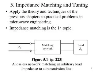
VCO Design Parameters: VTANK – tank voltage swing QTANK – tank quality factor JBIAS – current density C1:C2 – capacitance ratio LB – base inductance IBIAS – bias current Designing for Lowest Phase Noise Simulation Test Circuit
2. Optimum Current Density (JBIAS) OPTIMUM JBIAS OPTIMUM JBIAS = optimum noise current density (Jopt) of cascode.
3. Optimum Base Inductance (LB) Smallest LB results in Lowest Phase Noise
Maximize quality factor (Q) of resonant tank. Bias transistors at optimum noise current density Jopt. VCO Design Methodology Show a simulated plot of Jopt @ 40 GHz & fT, fMAX for cascoded transistor configuration
Choose smallest reproducible base inductance (LB). VCO Design Methodology (con’t) • Sweep IBIAS to minimize phase noise while choosing C1:C2 ratio to maximize VTANK while maintaining fosc. • Add inductive emitter degeneration LE. • [Li and Rein, JSSC 2003]
13 VCOs & Oscillators fabricated to examine the impact on phase noise of: Base inductance (LB) Accumulation-mode nMOS varactors versus. MIM capacitors Addition of LE Operation on 2nd harmonic versus. operation on fundamental. VCO Design Space Examined
Motivation VCO and BPSK transmitter circuit topologies Design methodology for lowest phase noise VCOs Experimental results Conclusions Outline
Jazz Semiconductor’s commercial SBC18 0.18 m BiCMOS process. Fabrication Technology • Peak fT and fMAX near 155 GHz. NFmin extracted from measured y-parameters [S. P. Voinigescu, et. al, JSSC 1997]
Family of 13 VCOs: Microphotographs Fundamental-Mode: (8) 35 GHz, (2) 60 GHz, Push-Push: (1) 70 GHz, (2) 120-GHz
65-GHz BPSK transmitter Microphotographs (con’t)
Averaged Spectral Plots for 35-GHz VCO (LB = 100 pH, with LE): 35-GHz VCO Measurements (A) VCO (B) Fixed Freq. Oscillator
Tuning and Output Power Characteristics: 35-GHz VCO Measurements (con’t)
Lowest Phase Noise Design Space Impact of: 1. Base Inductance 2. Inductive Emitter Degeneration (LE)
Averaged Spectral Plots: 60-GHz VCO Measurements (A) VCO (B) Fixed Freq. Oscillator
Measurements over Temperature: 60-GHz VCO Measurements (con’t)
Spectral Plots: Push-Push VCO Measurements • 70-GHz VCO • POUT > -14 dBm (b) 120-GHz VCO POUT > -30 dBm
Tuning Characteristics: Push-Push VCO Measurements (con’t)
*FOM = L{foffset} - 20log(fosc/foffset) + 10log(PDC/POUT) pp = push-push VCO Si-Based mm-wave VCO Comparison
With DATA (231-1 PRBS): BPSK Transmitter Measurements No DATA:
BPSK Transmitter Meas. (con’t) With DATA (27-1 PRBS pattern):
Motivation VCO and BPSK transmitter circuit topologies Design methodology for lowest phase noise VCOs Experimental results Conclusions Outline
Presented, with experimental validation, a systematic VCO design methodology for lowest phase noise. Compared to a MIM capacitor, accumulation-mode nMOS varactors degrades phase noise by 1-2 dB. Inductive degeneration lowers phase noise by 3-4 dB. Operation on 2nd harmonic increases tuning range by 50% - at expense of lower POUT First 65-GHz BPSK transmitter. Conclusions
Jazz Semiconductor, Gennum Corporation. Canadian Foundation for Innovation, Micronet, Canadian Microelectronics Corporation, NSERC. Marco Racanelli and Paul Kempf. Acknowledgements