Metrology Roadmap
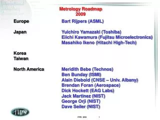
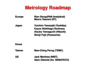
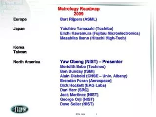
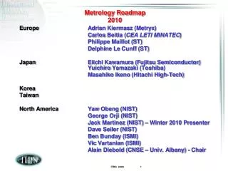
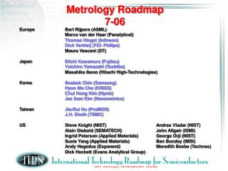
Metrology Roadmap. 2008. Metrology Roadmap 2008. Europe Thomas Hingst ( Qimonda ) Bart Rijpers (ASML) Japan Eiichi Kawamura (Fujitsu) Masahiko Ikeno (Hitachi High-Technologies) Yuichiro Yamazaki (Toshiba) Korea Chul Hong Kim ( Hynix ) Soobok Chin (Samsung)


Metrology Roadmap
E N D
Presentation Transcript
Metrology Roadmap 2008
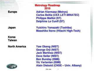
Metrology Roadmap2008 Europe Thomas Hingst (Qimonda) Bart Rijpers (ASML) Japan Eiichi Kawamura (Fujitsu) Masahiko Ikeno (Hitachi High-Technologies) Yuichiro Yamazaki (Toshiba) Korea Chul Hong Kim (Hynix) Soobok Chin (Samsung) Eun Sang Cho (DongbuHiTek) Taiwan North America Alain Diebold (CNSE – Univ. Albany) Meredith Beebe (Technos) Ben Bunday (ISMI) Dan Herr (SRC) Mike Garner (Intel) Steve Knight (NIST) Jack Martinez (NIST) Dave Seiler (NIST) Victor Vartanian (ISMI)
AGENDA • 2008 Changes • Lithography Metrology • FEP Metrology • Interconnect Metrology • ERM Metrology • Key Messages 2008 • Conclusions
Lithography Metrology for Advanced Patterning Spacer Patterning Double Exposure Double Patterning 2p CD p/2 Spacers Metrology Need: Latent Image CD CD-AFM after both exposures but no Solution for CD between exposures Metrology Need: Overlay with Precision of 70% Of Single Layer Metrology Need: Spacer Thickness on Sidewall Spacer Profile 22 nm Dense lines
Impact of Process on Metrology : courtesy Litho TWG Loading effects of etching and CVD depend on not only pattern environment but resist pattern shape. So the shape itself is important requirement of metrology. Requirements of shape should cover not only top CD, bottom CD, height and SWA, but 2D(or 3D) structure.
Metrology Challenges for Advanced Litho Processes 2 Population CD, SWA, height and pitch Potential Solution -> scatterometry Q: is there enough sensitivity for odd-even line scenario Metrology for Latent Image at 1st exposure might be avoided using AEC/APC approaches & CD/Overlay after double exposure
3D Metrology Requirements overlay shift creates asymmetry perfect overlay cross section example
New FEP Metrology Requirements for Ultimately Scaled and Functionally Enhanced CMOS: • Non-Destructive local strain/stress measurement • Dopant activation Metrology for USJ • Interface Metrology • New channel material or structures challenges • SiGe & III-V • Trigate FinFET, Nanowire • Carbon nanotubes & Graphene • Surface/film analysis on vertical surfaces • In-situ monitoring of multi-component oxides • In-Line work function measurements – band gap engineering for flash and gates • Active depth profile: what percentage of the implanted atoms/ions is electrically active? • FEP wants to measure particles and composition on bare silicon wafers and on in-process wafers down to 20nm size - non-destructive with high productivity
Cross sectioning Small laser spot for extracting single Tr. stress • Local Strain/Stress Measurement Proposal of new item on FEP table Relatively small laser spot (Visible light) with deeper penetration pMOS nMOS Ghani, et al (Intel) Wide laser spot for extracting average stress Measurement Point Stress Liner STI STI Channel Strain/Stress Modified from Fichtner’s figure
New table for Local Strain/Stress Measurementneed inputs from FEP and PIDS Table 120a Front End Processes Metrology Technology Requirements—Near-term Years Mobility Enhancement Factor For Idsat (Table 40ab) - Extended Planar Bulk - UTB FDS - DG Stress measurement with 50MPa resolution Spatial resolution (Offline, destructive, single Tr.) 1/5 of Gate Length Same size with HP Spatial resolution (Inline, non-destructive, Test pattern for average stress measurement) Using test pad of 100um X 100um Throughput (wafers/hour) (Inline, non-destructive, Test pattern) 25 sites per wafer
Local Strain/Stress Measurement Method (Tentative) Sensitivity Measurement Method Measurement Area Sample Thickness Area of Interest Stress Strain Transistor Level - CBED - NBD - TERS 20 MPa 100 MPa 50 MPa 0.02% 0.1% 0.05% 10-20nm ~10nm <50nm <100nm <300nm Destructive Destructive Destructive Non-Destructive Micro-Area Level 20 MPa 10 MPa 0.05% 0.01% ~150nm 100um - Confocal Raman - XRD - Photoreflectance Spectroscopy Non-Destructive Handling Area of ITRS Die - Die level flatness - Laser Interferometry - Coherent Gradient Sensing Non-Destructive Wafer - Laser Interferometry - Coherent Gradient Sensing 10 MPa 0.001% wafer Non-Destructive TERS (Tip Enhanced Raman Scattering) CBED (Convergent Beam Electron Diffraction) NBD (Nano Beam Electron Diffraction) XRD (X-ray Diffraction) * Stress – Strain relation : need to be clarified
Trend : Use Modeling to connect what you can measure with what you need to knowExample: Metrology of Strained Channel Devices MD Giles, et. al., VLSI Symposium 2004
Dopant profile measurement(Essentially destructive) • 2008 Update 10nm 10nm 10nm 1×10¹⁸atoms/cm3 Dan Herr - SRC Total throughput of analysis is one of remaining issues Do we need to put in a throughput requirement? What percentage of the atoms/ions is electrically active?
Wrap Around Gate FIN Wrap Around Gate Metrology Side Wall and Top Dielectric Thickness and Composition FINFET
Kreupl, Infineon • Carbon Nanotubes ? MARCO Center 2 mm Future Interconnect (ITRS 2008) • 3D Interconnect ? • Optical Interconnect ? Intel
2008 Interconnect Metrology • Existing Challenges • Measurements of Sidewall barrier thickness and continuity • Sidewall damage (compositional changes, densification and defect formation in low k) after etch remains a Major Gap - It will soon also be a Gap for FEP Metrology • Characterization of pores, pore size distribution, and topology • Detection of Voids after electroplating • Monolayer interface for new barrier-low k • Air Gap sacrificial layer does not require unique metrology • Metrology is needed for 3D Integration • TSV Depth and Profile through multiple layers • Alignment of chips for stacking – wafer level integration • Bond strength • Defects in bonding: un-bonded regions • Damage to metal layers; e.g., scratches which could result in voids • Defects in vias between wafers • CD determination of high aspect for Si vias • Wafer thickness and TTV after thinning • Defects after thinning including wafer edge • Characterization of the edge of graphene
ERD/Metrology Collaboration Discussion • Small geometrical metrologies, obtaining a reasonable signal/noise ratio – study, determine, and manage noise sources. Extract the signal from noise. • Issue of contamination of nano-scaled devices • Time resolved magnetic measurements. • Ability to perform real time measurements, e.g. phase transitions. • Wide band characterizations of rf devices – above 100 GHz. • Questions from Metrology • PCM – Near mfg? • MRAM – In production? Spin torque RAM • Contamination - • A requirements table is needed for on-line, in-line, and off-line metrology
Metrology Summary • FEP-Interconnect-Litho • 3D Metrology – Confirm Geometry Requirements e.g. film thickness on sidewall • Reference Methods for 3D • Stress – e.g. buried channels • ERD-ERM • Properties of low Dimensional Materials • Microscopy and feature size/function • Time resolved magnetic measurements • Ability to perform real time measurements, e.g. phase transitions High K changes Litho scaling & Metrology
Conclusions • CD Measurement improvements show a path to the 32/22 nm ½ Pitch • Transistor channel engineering requires Stress and Mobility Measurement • Interconnect requires Sidewall Measurements for barrier/seed and low trench • ERM and ERD require both improved imaging (such as aberration corrected TEM) and image simulation • Determination of not only atomic composition of layers, but electrical activity of those atoms/ions