ATmega128 Memory
ATmega128 Memory. (Flash memory, SRAM, EEPROM & I/O memory). ATmega128 Memory. AVR architecture has two main memory spaces Program memory : Flash memory Data memory : SRAM, EEPROM In-System Reprogrammable Flash Program Memory 128 Kbytes on-chip flash memory (ATmega128)

ATmega128 Memory
E N D
Presentation Transcript
ATmega128 Memory (Flash memory, SRAM, EEPROM & I/O memory)
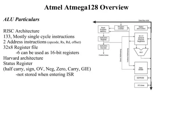
ATmega128 Memory • AVR architecture has two main memory spaces • Program memory : Flash memory • Data memory : SRAM, EEPROM • In-System Reprogrammable Flash Program Memory • 128 Kbytes on-chip flash memory (ATmega128) • Organized as 64K x 16 (since all instructions are 16 or 32 bits wide) • Divided into two sections • Boot Loader Program section • Application Program section
Flash Program Memory (cont’d) • Endurance : 10,000 write/erase cycles • Boot Program section is protected by Boot Lock bits (refer to p.277) • Flash memory programming is supported by SPI, JTAG, or Parallel Programming mode • Constant tables can be allocated within the entire program memory address space by using LPM (Load Program Memory) and ELPM (Extended Load Program Memory) instructions
SRAM Data Memory • Size : 4096 bytes (internal) up to 64Kbytes (external - optional) • Internal Data Memory : 4352 locations • First 32 locations for register file • Next 64 locations for standard I/O memory(can be accessed by I/O specific instructions or memory access instructions) • Next 160 locations for extended I/O memory(can be accessed by only memory access instructions -- LD/LDS/LDD, ST/STS/STD instructions) • Next 4096 locations for internal SRAM
Data Memory Map (up to 61184 x 8)
SRAM Data Memory (cont’d) • Optional external SRAM • Size : up to 61184 bytes (0x1100~0xFFFF : occupies the remaining address locations in the 64K address space) ≈ 60KBytes • Access time takes one additional clock cycle per byte compared to access of the internal SRAM
SRAM Data Memory (cont’d) • Addressing modes for data memory : • Direct (can reaches the entire data space) • Indirect with displacement • Indirect • Indirect with pre-decrement • Indirect with post-increment(X, Y, Z registers are used for automatic pre-decrement and post-increment)
SRAM Data Memory (cont’d) • On-chip data memory access time : two CPU clock cycles
EEPROM Data Memory • Size : 4K bytes • Address space : separate from SRAM • Endurance : 100,000 write/erase cycles • EEPROM programming (write) time : 8.5 ms • Access(read/write) operation can be done by CPU through the following registers : • EEPROM Address Register • EEPROM Data Register • EEPROM Control Register
EEPROM Data Memory (cont’d) • EEPROM Address Register (EEAR) • BIT 15..12 : reserved bits • BIT 11..0 : EEPROM address (4096 bytes) : $1F($3F) : $1E($3E)
EEPROM Data Memory (cont’d) • EEPROM Data Register(EEDR) • BIT 7..0 : EEPROM data : $1D($3D)
EEPROM Data Memory (cont’d) • EEPROM Control Register(EECR) • BIT 7..4 : reserved • BIT 3 : EERIE (EEPROM Ready Interrupt Enable) • BIT 2 : EEMWE (EEPROM Master Write Enable) • BIT 1 : EEWE (EEPROM Write Enable) • BIT 0 : EERE (EEPROM Read Enable) : $1C($3C)
EEPROM Data Memory (cont’d) • Procedure for EEPROM write operation • Wait until EEWE becomes 0 (previous write is complete) • Write new EEPROM address to EEAR • Write new EEPROM data to EEDR • Write a logical 1 to EEMWE bit while writing 0 to EEWE in EECR • Write a logical 1 to EEWE bit (within 4 clock cycles after setting EEMWE)
I/O Memory • All I/Os and peripherals are placed in the I/O space • All I/O locations are accessed by LD/LDS/LDD and ST/STS/STD instructions : transfer data between 32 working registers and I/O registers (in this case, addresses are added by $20 $20~$FF: memory-mapped I/O) • I/O registers within the address range $00 ~ $3F can be accessed by using IN and OUT instructions (Isolated I/O) • I/O registers within the address range $00 ~ $1F • directly bit-accessible using SBI and CBI instructions • value of single bit can be checked by using SBIS and SBIC instructions • Extended I/O space ($60 ~ $FF) can be accessed only by LD/LDS/LDD and ST/STS/STD instructions
External Memory Interface • When the External Memory(XMEM) is enabled, address space outside the internal SRAM becomes available using the dedicated External Memory pins (Port A: AD7:0; Port C: A15:8; Port G: ALE, RD/, WR/).
Data Memory Map (up to 61184 x 8)