Download
1 / 24
240 likes | 261 Vues
This talk focuses on the technical aspects of the development and prototyping of the STAR pixel detector. It covers the detector requirements, characteristics, design choices, mechanical design, readout development, and sensor development.

E N D
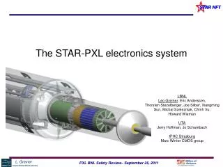
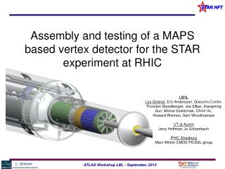
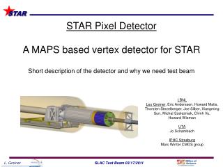
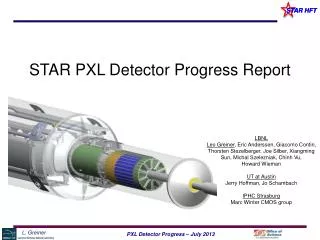
STAR Pixel DetectorA MAPS based vertex detector for STARwith status of development and prototyping LBNL Leo Greiner, Eric Anderssen, Howard Matis, Thorsten Stezelberger, Joe Silber, Xiangming Sun, Michal Szelezniak, Chinh Vu, Howard Wieman UTA Jo Schambach IPHC Strasburg Marc Winter CMOS group
Talk Outline The primarily focus of this talk is technical. • STAR Upgrades at RHIC. • Pixel detector requirements and design. • Detector characteristics. • Detector Development and Prototyping. • Summary and plans.
Vertex Detector Motivation • Direct Topological reconstruction of Charm • Detect charm decays with small c, including D0 K Method: Resolve displaced vertices (100-150 microns)
Inner Detector Upgrades TPC – Time Projection Chamber (main detector in STAR) HFT – Heavy Flavor Tracker • SSD – Silicon Strip Detector • r = 22 cm • IST – Inner Silicon Tracker • r = 14 cm • PXL – Pixel Detector • r = 2.5, 8 cm We track inward from the TPC with graded resolution: ~1mm ~300µm ~250µm <30µm vertex TPC SSD IST PXL
Detector Requirements and Characteristics • -1 ≤ Eta ≤ 1, full Phi coverage (TPC coverage) • ≤ 30 µm DCA pointing resolution required for 750 MeV/c pion • Two or more layers with a separation of > 5 cm. • Pixel size of ≤ 30 µm • Radiation length as low as possible but should be ≤ 0.5% / layer (including support structure). The goal is 0.37% / layer • ~200-300 hits / sensor (inner layer, 4 cm2) in the integration time window (at operating point chosen). • Survive radiation environment at the level (projected) of 20 to 90 k Rad /year and 2 x 10¹¹ - 1012/cm2 Neq /year. • MAPS Pixel technology • Sensor power dissipation ~170 mW/cm2 • Sensor integration time <200 μs (L=8×1027) • Thinned silicon sensors (50 μm thickness) • Air cooling • Quick extraction and detector replacement Requirements Design Choices
Aluminum conductor Ladder Flex Cable PXL Detector Mechanical Design Cabling and cooling infrastructure Mechanical support with kinematic mounts (insertion side) carbon fiber sector tubes (~ 200um thick) Insertion from one side 2 layers 5 sectors / half (10 sectors total) 4 ladders/sector Ladder with 10 MAPS sensors (~ 2×2 cm each) 20 cm
PXL Detector Basic Unit (RDO) 6 m (24 AWG TP) 2 m (42 AWG TP) Clk, config, data Clk, config, data, power Mass Termination Board + latch-up protected power daughter-card 100 m (fiber optic) PXL built events RDO PC with DDL link to RDO board • Highly parallel system • 4 ladders per sector • 1 Mass Termination Board (MTB) per sector • 1 sector per RDO board • 10 RDO boards in the PXL system RDO motherboard w/ Xilinx Virtex-5 FPGA
Detector Characteristics 356 M pixels on ~0.16 m2 of Silicon
Detector Development Path Phase-1 prototype Final sensor prototype Pre-production prototype Sensor development Binary readout of all pixels Phase-1 Ladder readout Final individual readout Final Ladder readout Readout development Probe tests Probe tests Infrastructure development 10 sensor FR-4 prototype 10 sensor kapton prototype 10 sensor Al+ kapton prototype Cable development Cooling & vibration simulation Cooling & vibration testing Phase-1 Sector prototype Final Sector prototype Mechanical development Prototype detector Final detector Deliverable
Detector Development Path Phase-1 prototype Final sensor prototype Pre-production prototype Sensor development Binary readout of all pixels Phase-1 Ladder readout Final individual readout Final Ladder readout Readout development Probe tests Probe tests Infrastructure development 10 sensor FR-4 prototype 10 sensor kapton prototype 10 sensor Al+ kapton prototype Cable development Cooling & vibration simulation Cooling & vibration testing Phase-1 Sector prototype Final Sector prototype Mechanical development Prototype detector Final detector Deliverable
Sensor Development with IPHC The following descriptions are terse. Please see A. Dorokhov talk on Thursday • Final Sensor • Reticle size (~ 4 cm²) • Pixel pitch 20.7 μm • 928 x 960 array ~890 k pixels • Reduced power dissipation • Vdd: 3.0 V • Estimated power consumption ~134 mW/cm² • Short integration time 185.6 μs • Optimized discriminator timing • Improved threshold uniformity • on-chip zero suppression • 2 LVDS data outputs @ 160 MHz • High Res Si option – significantly increases S/N and radiation tolerance. • Phase-1 prototype • Reticle size (~ 4 cm²) • Pixel pitch 30 μm • 640 x 640 array ~ 410 k pixels • Column parallel readout • Column discriminators • Binary readout of all pixels • Data multiplexed onto 4 LVDS outputs @ 160 MHz • Integration time 640 μs • Functionality tests and yield look very good. • Measured ENC is 15 e-.
Readout Development Ladder- ITB Prototyped Mass Termination Board – Prototyped and in use Readout Board – Prototyped and in use System firmware and software – Prototyped and in use • System architecture validated with 160 MHz data path testing. (BER < 10-14) • Prototype RDO system (hardware, firmware and software) is in use for sensor characterization, probe testing and ladder prototype testing. • RDO hardware is the same for both sensor generations, only the firmware changes.
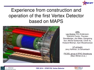
PXL Ladder Structure Each PXL ladder consists of three main elements 10 x sensors adhesive Kapton flex cable adhesive Carbon fiber stiffener plate • Thinning sensors to 50 µm is a standard commercial process. • The adhesive is a 50 µm acrylic film adhesive. • The carbon fiber stiffener plate is a basket weave 90º prepreg. • The flex cable is the component that requires a significant development effort.
Flex Cable Development Hybrid Copper / Aluminum conductor flex cable Preliminary design Side view (exaggerated vertical scale) Top View Low mass region calculated X/X0 for Al conductor = 0.073 % Low mass region calculated X/X0 for Cu conductor = 0.232 % PXL Cable development is planned as a 4 stage process: • Infrastructure testing board (large and configurable FR-4 ladder prototype). • - Validate design concepts and determine envelope of sensor operation. • Prototype detector cable FR-4 with Cu traces. • Prototype detector cable Kapton with Cu traces. • Prototype detector cable Kapton with Al traces.
Infrastructure test board • The ITB testing is effectively a ladder level system test with full thickness sensors. • complete chain of RDO system (MTB, RDO, long cables) at full system speed of 160 MHz. • Multi-drop clock working. • JTAG daisy chain working. • 10 sensor synchronization working. • Fully automated testing with working RDO. preliminary • The noise coupling mechanism is under investigation. • An ITB with thinned 50 µm sensors is ready for testing. • Design of the next stage (FR-4 form factor size) will begin soon.
Mechanical Development The CTE difference between silicon, carbon and the kapton ladder cable is a potential source of thermally induced deformation. FEA simulations give a maximum ΔT of 20° C Air-flow based cooling system for PXL to minimize material budget. ladder region • Silicon power: tested at 170 mW/cm2 (~ power of sunlight) • 350 W total in the ladder region (Si + drivers) Detector mockup to study cooling efficiency computational fluid dynamics
Mechanical Development Sensor section ~20 cm Driver section ~ 6 cm • Kapton cables with copper traces forming heaters allow us to dissipate the expected amount of power in the detector • 6 NTC thermistors on each ladder • Sector 1 was equipped with 10 thinned dummy silicon chips per ladder with Pt heaters vapor deposited on top of the silicon and wire bonded to heater power. Thermal camera image of sector 1 (composite image): Power ~340 W Airflow 10.1 m/s
Mechanical Development unsuported end mid-section fixed end Solid – inner layer Open – outer layer • Measurement results agree with simulations and meets calculated stability envelope tolerance. • Air flow-induced vibrations (< 10 m/s) are within required stability window.
Summary and future plans • We have a well advanced mechanical design that is in the process of being verified by simulation and prototyping. • The prototype RDO system is performing well. • Sensor development with IPHC is on schedule and we expect the first prototype final sensor delivery in Q1 2011. • The ladder cable development is on schedule and we are evaluating the ITB performance with the full compliment of 10 working sensors. • We expect to have our DOE CD-2/3 review in January of 2011 (release of funding for full detector construction). • Detector installation is scheduled for 2013.
Probe testing thinned sensors Probe testing on diced and thinned (50μm) sensors – to meet yield requirements • Dedicated probe pads in the sensor pad ring. • Up to 3 probe tests on a sensor. • Automated test system based on the prototype RDO system gives a qualitative analysis of probed sensors including identification of dead/stuck pixels/columns. • 1st wafer of thinned sensors under test. Vacuum chuck for probe testing 20 (50 μm thick) MAPS sensors per testing session. Sensor Yield >90% Thinning (individual method) yield => >90% Thinning (pre-scribe method) initial yield => ~70%* * Expected yield is >90%
Simple Data Rate PXL System • Data rate to storage = 199 MB/sec (1kHz trigger) • 199 kB / event
Sensor generation and RDO attributes ADC CDS Data sparsification readout to DAQ Pixel Sensors CDS Disc. The sensor and readout development are strongly coupled Complementary detector readout digital signals analog signals digital analog MimoSTAR sensors 4 ms integration time 1 2 Phase-1 sensors 640 μs integration time 3 PXL final sensors (Ultimate) < 200 μs integration time Sensor and RDO Development Path
RDO System Design – Physical Layout Sensors / Ladders / Sectors (interaction point) RDO Boards 1-2 m Low mass twisted pair LU Protected Regulators, Mass cable termination Platform 30 m Power Supplies 6 m - twisted pair 30 m 100 m - Fiber optic Control PCs 30 m DAQ Room DAQ PCs (Low Rad Area)