Download
1 / 24
370 likes | 1.26k Vues
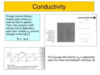
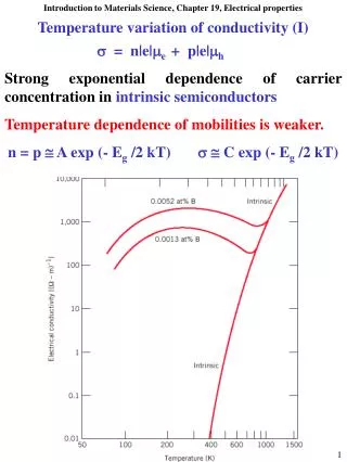
Temperature variation of conductivity (I). = n|e| e + p|e| h Strong exponential dependence of carrier concentration in intrinsic semiconductors Temperature dependence of mobilities is weaker. n = p A exp (- E g /2 kT) C exp (- E g /2 kT).

E N D
Temperature variation of conductivity (I) = n|e|e + p|e|h Strong exponential dependence of carrier concentration in intrinsic semiconductors Temperature dependence of mobilities is weaker. n = p A exp (- Eg /2 kT) C exp (- Eg /2 kT)
Temperature variation of conductivity (II) n = p A exp (- Eg /2 kT) C exp (- Eg /2 kT) Plotting log of , p, or n vs. 1/T produces a straight line. Slope is Eg/2k; gives band gap energy. ln(n) = ln(p) ln(A) - Eg /2 kT
Temperature variation of conductivity (III) • Extrinsic semiconductors • low T: all carriers due to extrinsic excitations • mid T: most dopants ionized (saturation region) • high T: intrinsic generation of carriers dominates
Semiconductor Devices. Diode (I) Diode allows current flow in one direction only p-n junction diode: adjacent p- and n-doped semiconductor regions Positive side of a battery is connected to p-side (forward bias): large amount of current flows. Holes and electrons pushed into junction region, where they recombine (annihilate).
Semiconductor Devices. Diode (II) If the polarity of the voltage is flipped, the diode operates under reverse bias. Holes and electrons are removed from the region of the junction, which therefore becomes depleted of carriers and behaves like an insulator.
Semiconductor Devices. Diode (III) Reverse bias: holes and electrons are drawn away from junction. Junction region depleted of free carriers current is small.
Semiconductor Devices. Diode (IV) Asymmetric current-voltage characteristics of diode converts alternating current to direct current (rectification).
Transistors. Used to amplify electric signal and Switching devices in computers. Two major types Junction (or bimodal) transistor MOSFET transistor. p-n-p (or n-p-n) junction transistor contains two diodes back-to-back. The Central region (base) is thin (~ 1 micron or less) and is sandwiched in between emitter and collector
Junction transistor Emitter-base junction is forward biased: holes are pushed across junction. Some recombine with electrons in the base, but most cross the base as it is thin. They are then swept into the collector. A small change in base-emitter voltage causes a relatively large change in emitter-base-collector current. Hence a large voltage change across output (“load”) resistor - voltage amplification
Junction transistor Emitter-base junction is forward biased, base-collector junction is reverse biased. Thus, the base of the PNP transistor must be negative with respect to the emitter, and the collector must be more negative than the base.
PNP Forward-biased junction Forward biased emitter-base junction, positive terminal of battery repels emitter holes toward base, while negative terminal drives base electrons toward emitter
PNP junction interaction In reverse-biased junction: negative voltage on collector and positive voltage on base blocks majority current carriers from crossing junction. Increasing forward-bias voltage of transistor reduces emitter-base junction barrier. This allows more carriers to reach the collector, causing an increase in current flow from emitter to collector and through external circuit.
MOSFET (Metal-Oxide-Semiconductor Field Effect Transistor) MOSFET transistor: two small islands of p-type semiconductor created within n-type silicon substrate. Islands connected by narrow p-type channel. Metal contacts are made to islands (source and drain), one more contact (gate) is separated from channel by a thin (< 10 nm) insulating oxide layer. Gate serves the function of the base in a junction transistor (electric field induced by gate controls current through the transistor)
MOSFET (Metal-Oxide-Semiconductor Field Effect Transistor) Voltage applied from source encourages carriers (holes in the case shown below) to flow from the source to the drain through the narrow channel. Width (and hence resistance) of channel is controlled by intermediate gate voltage. For example, if positive voltage is applied to the gate, most of the holes are repelled from the channel and conductivity is decreasing. Current flowing from the source to the drain is therefore modulated by the gate voltage (amplification and switching)
Transistors and microelectronic devices • MOSFET dominates microelectronic industry (memories, microcomputers, amplifiers, etc.) • Large Si single crystals are grown and purified. Thin circular wafers (“chips”) are cut from crystals • Circuit elements are constructed by selective introduction of specific impurities (diffusion or ion implantation) • A single 8” diameter wafer of silicon can contain as many as 1010 - 1011 transistors in total • Cost to consumer ~ 0.00001c each.
Conduction in Polymers and Ionic Materials Ionic Materials • The band gap is large and only very few electrons can be promoted to the valence band by thermal fluctuations • Cation and anion diffusion can be directed by the electric field and can contribute to total conductivity: total = electronic + ionic • High temperatures produce Frenkel and Schottky defects which result in higher ionic conductivity. Polymers • Polymers are typically good insulators but can be made to conduct by doping. • A few polymers have very high electrical conductivity - about one quarter that of copper, or about twice that of copper per unit weight.
Capacitance Voltage V applied to parallel conducting plates plates charged by +Q, –Q electric field E develops between plates + + + + + Charge can remain even after voltage removed. - - - - - - Ability to store charge capacitance C = Q / V [Farads] C depends on geometry of plates and material between plates C = r o A / L = A / L A is area of plates, L is distance between plates, is permittivity of dielectric medium, o is permittivity of a vacuum (8.85x10⁻¹² F/m2), and r is relative permittivity (dielectric constant) of material, r = / o = C / Cvac
Dielectric Materials Dielectric constant of vacuum is 1 and is close to 1 for air and many other gases. When piece of dielectric material is placed between two plates capacitance can increase significantly. C = r o A / L with r = 81 for water, 20 for acetone, 12 for silicon, 3 for ice, etc. Dielectric is insulator in which electric dipoles are induced by electric field d _ _ _ + + + _ + Magnitude of electric dipole moment is p = q d
Dielectric Materials Dipole orientation along electric field in the capacitor causes charge redistribution. Surface nearest to the positive capacitor plate is negatively charged and vice versa. net negative charge at the surface, -Q’ Q0 + Q’ + + + + + + + + - + - + - + - + - + - + - + - + region of no net charge P - + - + - + - + - + - + - + - + - + - + - + - + - + - + - + - + net negative charge at the surface, Q’ = PA - - - - - - - - - -Q0 - Q’ Dipole alignment extra charge Q’ on plates: Qt = |Q+Q’| now C = Qt / V Increased capacitance r = C / Cvac > 1 Dipole formation/alignment in electric field is called polarizationP = Q’/A
Dielectric Materials Surface charge density (also called dielectric displacement) is D = Q/A = r oE = oE + P Polarization is responsible for the increase in charge density above that for vacuum • Mechanisms:dipole formation/orientation • electronic (induced) polarization: Electric field displaces negative electron “clouds” with respect to positive nucleus. • Ionic materials (induced) polarization: Applied electric field displaces cations and anions in opposite directions • molecular (orientation) polarization: Some materials possess permanent electric dipoles (e.g. H2O). In absence of electric field, dipoles are randomly oriented. Applying electric field aligns these dipoles, causing net (large) dipole moment. Ptotal = Pe + Pi + Po
Mechanisms of Polarization electronic polarization ionic polarization molecular (orientation) polarization
Dielectric Strength Breakdown: high electric fields (>108 V/m) excite electrons to conduction band + accelerate them to high energies they collide with and ionize other electrons Avalanche process (or electrical discharge). Field necessary is called dielectric strength or breakdown strength. Piezoelectricity (some ceramic materials) Application of a force electric field (polarization) and vice-versa Piezoelectric materials convert mechanical strain into electricity (microphones, strain gauges, sonar detectors) Piezoelectric materials include barium titanate BaTiO3, lead zirconate PbZrO3, quartz.
Nanoscopic materials design The Center for Nanoscopic Materials Design at UVa http://www.mrsec.virginia.edu/
Summary Make sure you understand language and concepts: • Acceptor state • Capacitance • Conduction band • Conductivity, electrical • Dielectric constant • Dielectric displacement • Dielectric strength • Diode • Dipole, electric • Donor state • Doping • Electrical resistance • Electron energy band • Energy band gap • Extrinsic semiconductor • Fermi energy • Forward bias • Free electron • Hole • Insulator • Intrinsic semiconductor • Ionic conduction • Junction transistor • Matthiessen’s rule • Metal • Mobility • MOSFET • Ohm’s law • Permittivity • Piezoelectric • Polarization • Polarization, electronic • Polarization, ionic • Polarization, orientation • Rectifying junction • Resistivity, electrical • Reverse bias • Semiconductor • Valence band