TDC and ADC Implemented Using FPGA
TDC and ADC Implemented Using FPGA. Wu, Jinyuan Fermilab, PPD/EED Feb. 2007. Introduction. FPGA devices are considered belonging to digital world while ADC is an analog measurement function. ADC can be implemented directly with FPGA plus a few passive (resistors and capacitors) components.

TDC and ADC Implemented Using FPGA
E N D
Presentation Transcript
TDC and ADC Implemented Using FPGA Wu, Jinyuan Fermilab, PPD/EED Feb. 2007
Introduction • FPGA devices are considered belonging to digital world while ADC is an analog measurement function. • ADC can be implemented directly with FPGA plus a few passive (resistors and capacitors) components. • Bench tests are done for ADC 6-bit@22.5 MHz and 9-bit@2MHz. Other speed/resolution combinations are possible. • The ADC is based on ramp & compare with TDC implemented inside FPGA with 0.69 ns LSB (200ps RMS). • More than 32 channels of TDC are tested in Altera Cyclone (EP1C6Q240C6, $20) devices.
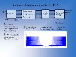
FPGA ADC Using FPGA AMP & Shaper ADC AMP & Shaper ADC • Analog signals from AMP & Shapers are directly fed to FPGA pins. • FPGA output and passive RC network are used to generate ramping reference voltage VREF. • The input voltages and VREF are compared using FPGA differential input receiers. • The times of transitions representing input voltage values are digitized by TDC blocks in FPGA. AMP & Shaper ADC AMP & Shaper ADC FPGA AMP & Shaper TDC AMP & Shaper TDC AMP & Shaper TDC AMP & Shaper TDC V1 V2 V3 VREF R1 R1 V4 C T1 T2 T3 T4 R2
Data In Q3 QF c0 c0 QE Q2 c90 QD Q1 c180 Q0 c90 c270 Multiple Sampling Clock Domain Changing DV T0 T1 Trans. Detection & Encode Coarse Time Counter TS TDC Using FPGA (LSB 1ns+-) 4x Sampling: 250 MHz: 1ns(LSB), 288ps(RMS) 400 MHz: 625ps(LSB), 180ps(RMS)
Clock Domain Changing TDC Inside FPGA Multiple Sampling Q3 QF • Sampling rate: 360 MHz x4 phases = 1.44 GHz. • LSB = 0.69 ns. • Logic elements with critical timing are assigned as shown. c0 c0 QE Q2 c90 QD Q1 c180 Q0 c90 c270 DV T0 T1 Trans. Detection & Encode 4Ch Coarse Time Counter TS Logic elements with non-critical timing are freely placed by the fitter of the compiler.
Bench Test of TDC RAM Flash RAM FPGA eZ80 TDC 45MHz Micro-processor address line driven by 45 MHz clock. 32 TDC bin = 1 clock cycle (0.69ns LSB) RAM Flash RAM FPGA eZ80 TDC 45MHz Micro-processor data line. Data out from different sources.
Differential Nonlinearity FPGA Quasi-random Input TDC The “beat” between input and 45MHz. 45MHz The placement above gives even bin width. Occupancy for each bin should 25%. The residual DNL < 690*(26-22)/25 = 110ps
ADC: Discharge Curve Reference: V-T Curve FPGA TDC TDC VREF • The differential receivers are nearly rail-to-rail comparators, but perform best from 0.5-2.2V. • Measurement range: 9 bits: • Ramping time 512x0.69ns = 353ns. • >2MHz sampling rate. • Dynamic range: about 12 bits: • 1.6mV/ns or 1.1mV/LSB @ 350ns. • 2.2V/1.1mV ~ 212. 50 270pF 511 t = 146 ns
ADC Test: Reference on BD3_19 FPGA TDC TDC VREF 50 50 t = 59 ns 1000pF 100 • Longer time constant causes the V-T curve to be nearly linear. • Sampling rate: 22.5MHz (2/88ns). • Measurement range: 6 bits. • Sensitivity: 10mV/LSB.
ADC Test: Waveform Digitization on BD3_19 Input Waveform Converted Raw Data Input Waveform, Overlap Trigger
ADC Test: Reference on BD4_22 FPGA TDC TDC VREF 50 50 150pF t = 7.5 ns 100 • Shorter time constant causes the V-T curve to be exponential. • Sampling rate: 22.5MHz (2/88ns). • Measurement range: 6 bits. • Sensitivity < 6mV/LSB. • Dynamic Range: ~8 bits.
ADC Test: Waveform Digitization on BD4_22 Raw Data Small pulses are emphasized by the trailing ramp measurement. Input Waveform The data measured by trailing ramp is much more smoother than the leading ramp for small pulses. Converted
Notes • Like in any analog circuits, noise reduction is the key to reach good resolution. Two primary measures are taken: • Appropriate arrangement of the grounding for analog signals. • Microprocessor are put in “wait” state during ramping and comparing. • Large noise due to single ended TTL are bad. But small and random noise from differential outputs can be good for “dithering”. This is to be studied. • Being non-linear, the RC exponential charging curve is bad. But it allows expansion of dynamic range, which is good. The conversion to linear scale in FPGA is very simple.
Remarks • The ADC functions tested have met requirements of many applications in high energy physics and accelerator instrumentation. • The FPGA ADC will not completely replace commercial ADC or ASIC. But it is appealing for sake of convenience (like for slow control/monitoring) or for low cost with large channel count (like for straw tube or TPC chambers).
Beyond • The TDC-readout system has excessive capabilities. Don’t hastate to ask more if you need. • TDC: Arrival time + pulse width. • Chamber info in trigger.
TDC FPGA (32 Ch) 4Ch
The FPGA TDC Test Card Shown here is Fermilab Beam Loss Monitor (BLM) Control Card VME Interface (As hit input) FPGA Serial Port Microprocessor
AMP Cards TDC Cards Readout Cards TDC-Readout System
TDC TDC Readout Card TDC TDC TDC TDC TDC TDC TDC TDC TDC TDC TDC TDC TDC TDC CC DD SD SC RJ45 A A7 A6 A5 A4 A3 A2 A1 A0 CC DD SD SC RJ45 B B7 B6 B5 B4 B3 B2 B1 B0
D0 D1 Error Detect TS Header CCx1 clr D1 Decoder load EV CC inc clr D0 CCx4 • CC = plain 26.5MHz clock most of time. • On start, send marker D0 to reset TS and EV counters. • For L1 trigger, send D1, TS and EV are stored into header. • TS is mod 294 (super bunch?). • Every 294 cycles, send D1 for TS error checking. • The header contains TS and EV so that EV errors can be detected offline.