Download
1 / 36
390 likes | 575 Vues
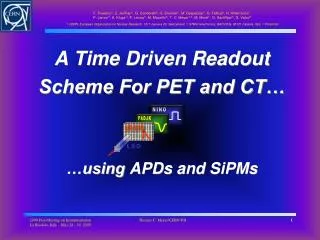
A Time Driven Readout Scheme For PET and CT… …using APDs and SiPMs. NINO. NINO. NINO. NINO. PADJK. PADJK. PADJK. PADJK. APD Array. APD Array. APD Array. APD/SiPM. LSO. LSO. LSO. LSO. Fig. 5: Functional diagram of the photon detection and signal processing layout.

E N D
A Time Driven Readout Scheme For PET and CT……using APDs and SiPMs NINO NINO NINO NINO PADJK PADJK PADJK PADJK APD Array APD Array APD Array APD/SiPM LSO LSO LSO LSO Fig. 5: Functional diagram of the photon detection and signal processing layout Fig. 5: Functional diagram of the photon detection and signal processing layout F. Powolny1), E. Auffray1), G. Condorelli2), S. Brunner1), M. Despeisse1), G. Fallica2), H. Hillemanns1), P. Jarron1), A. Kluge1), P. Lecoq1), M. Mazzillo2), T. C. Meyer1,3), M. Morel1), D. Sanfillipo2), G. Valvo2) 1) CERN, European Organization for Nuclear Research, 1211 Geneva 23, Switzerland, 2) STMicroelectronics, R&D DSG, 95121 Catania, Italy, 3) Presenter Thomas C. Meyer/CERN-PH 1
Outline of Presentation • Why a new readout technique? 2005 Thomas C. Meyer/CERN-PH
Outline of Presentation • Why a new readout technique? • The “Time Based” approach. 2005 2006 Thomas C. Meyer/CERN-PH
Outline of Presentation • Why a new readout technique? • The “Time Based” approach. • APD detector & TB readout. 2005 2006 2007 Thomas C. Meyer/CERN-PH
Outline of Presentation • Why a new readout technique? • The “Time Based” approach. • APD detector & TB readout. • TOF capability? 2005 2006 2007 2008 Thomas C. Meyer/CERN-PH
Outline of Presentation • Why a new readout technique? • The “Time Based” approach. • APD detector & TB readout. • TOF capability? • SiPMs and TB readout. 2005 2006 2007 2008 2009 Thomas C. Meyer/CERN-PH
Outline of Presentation • Why a new readout technique? • The “Time Based” approach. • APD detector & TB readout. • TOF capability? • SiPMs and TB readout. • Summary. 2005 2006 2007 2008 2009 Thomas C. Meyer/CERN-PH
Why a New Readout? • Clinical goals: • Multimodality: CT, PET, MRI, US, ... • Reduce patient exposure time; • Compensate for patient/organ motion; • Facilitate image fusion (PET/CT); • Simultaneous imaging of tumor response and responsiveness, as well as dose delivery in vivo. PHILIPS GEMINI TF™ Thomas C. Meyer/CERN-PH
Why a New Readout? • Clinical goals: • Multimodality: CT, PET, MRI, US, ... • Reduce patient exposure time; • Compensate for patient/organ motion; • Facilitate image fusion (PET/CT); • Simultaneous imaging of tumor response and responsiveness, as well as dose delivery in vivo. • Technical goals (“From HEP to PET”): • Use technologies & techniques devel’d for HEP • State-of-the-art electronics; • Compact and reliable data processing; • System integration and cost. PHILIPS GEMINI TF™ CERN CMS Thomas C. Meyer/CERN-PH
Why “Time” Based? • Leads to simple readout architectures: • Only digital pulses ⇒ simple electronics • No flash ADCs (running at > 500MHz, power) • Simple timing circuits: • Need only discriminators and TDCs; • Derive time and energy information from one digital pulse. • Time over threshold (T.o.T.), pulse width modulation; • Build on in-house experience from large experiments. Thomas C. Meyer/CERN-PH
Time Based Readout: How? i(t) P.A. Discr. V(t) NINO FEDC05 t Threshold i(t) V(t) t Thomas C. Meyer/CERN-PH
Time Based Readout: How? i(t) P.A. Discr. V(t) NINO LSO-like Test Pulse FEDC05 t Threshold i(t) V(t) t Time Walk Thomas C. Meyer/CERN-PH
Time Based Readout: How? i(t) P.A. Discr. V(t) NINO LSO-like Test Pulse FEDC05 t Threshold i(t) V(t) t Time Walk Thomas C. Meyer/CERN-PH
Time Based Readout: How? i(t) P.A. Discr. V(t) NINO LSO-like Test Pulse FEDC05 t Non-Linearity Correction Threshold i(t) V(t) Pulse Width Time Walk Correction t Time Walk Timestamp from leading edge after time walk correction. Photon energy from falling edge (pulse width). Need only discriminator and TDC for both. Thomas C. Meyer/CERN-PH
APD Detector w/ LHC-Electronics SIXTH FRAMEWORK PROGRAMME PRIORITY 1 FP6-2002 LIFESCIHEALTH Proposal 505785 i(t) V(t) i(t) P.A. Discr. NINO (ALICE - TOF) Hamamatsu S8550 FEDC05 (ATLAS) LSO APD • FEDC05 chip: • Preamplifier developed for ATLASSilicon Tracker • 400 electrons ENC (r.m.s.) • Gain = 4mV/fC • 16 channels • 13ns peaking time NINO FEDC05 APD (2 x 2 x 10 mm3) LSO NINO APD 22Na-Source FEDC05 • NINO chip: • Very fast discriminator (3GHz BW) • Signal peaking time: <1ns • Output time jitter: ≤ 25ps • 8 channels • Power consumption: 27mW/ch. Thomas C. Meyer/CERN-PH
The NINO Chip Vdd R R M6 M7 TH+ TH- Out1+ Vdd Out1 - 2.50 2.20 M5 M0 Out A2 + 2.30 Out A1 + 2.10 R R 2.10 BiasN3 Inth1 Inth2 BiasN2 threshold 1.90 2.00 1.70 OutA- OutA+ M4 M1 Out A2 - Out A1 - 1.50 1.90 0 5ns 10ns In+ 0 5ns 10ns In- M6 M7 InA- InA+ time [s] time [s] Vout + BiasN1 2.60 2.60 Out1 + Out A1 + Out A2 + Out A3 + Out A4 + In + Input stage M3 M2 2.30 Out A4 + 2.30 Out A3 + x6 x6 x6 x6 M8 BiasN5 2.00 2.00 In - Out A3 - 1.70 1.70 Out1 - Out A1 - Out A2 - Out A4 - Out A3 - Out A4 - 1.40 1.40 Cascade amplifier Vout - 0 5ns 10ns 0 5ns 10ns time [s] time [s] 4 Cascaded amplifiers Output buffer Thomas C. Meyer/CERN-PH
“SPICE” of Readout Chain i(t) V(t) i(t) P.A. Discr. NINO (ALICE - TOF) Hamamatsu S8550 FEDC05 (ATLAS) APD LSO-APD Pulses FEDC05 Output NINO output (+) Time Stamp Energy Thomas C. Meyer/CERN-PH
Energy Resolution & Dynamic Range With APDs & NINO 122keV 57Co 176Lu Background 122keV 176Lu Background 22Na Raw data[Pulse Width] 511keV Look-up Table 511keV Corrected data[Charge/Energy] Linearity after correction Energy resolution 22Na 1275keV 22Na 137Cs 57Co 1275keV Thomas C. Meyer/CERN-PH
Timing Resolution With APDs & NINO • How “fast” are APDs in the time encoded ‘NINO’ setup? • What are the limitations? • What are the alternatives? • The road to TOF-PET… Thomas C. Meyer/CERN-PH
Timing Resolution With PMT (Reference) 470ps FWHM No corrections applied; CFD is free of Time Walk. Thomas C. Meyer/CERN-PH
Timing Resolution With PMT–APD Photo-peak Selection And Time Walk Correction on APD Setup 470ps FWHM 1180ps FWHM Thomas C. Meyer/CERN-PH
Timing Resolution With Dual APD Photo-peak Selection And Time Walk Correction on both APD Setups 470ps FWHM 1180ps FWHM Raw data 1600ps FWHM After photo-peak selection + Time walk correction Thomas C. Meyer/CERN-PH
Time Jitter of Detector and Readout NINO PADJK [ps] rms [ps] FWHM [%] Front end electronics noise together with the APD dark current contribute ~ 20% to the total time jitter. Thomas C. Meyer/CERN-PH
Time Jitter of Detector and Readout NINO PADJK APD [ps] rms [ps] FWHM [%] Front end electronics noise together with the APD dark current contribute ~ 20% to the total time jitter. Non-uniformities in avalanche amplification in the APD account for ~ 30%. Thomas C. Meyer/CERN-PH
Time Jitter of Detector and Readout NINO PADJK APD [ps] rms [ps] FWHM LSO [%] • Front end electronics noise together with the APD dark currentcontribute ~ 20% to the total time jitter. • Non-uniformities in avalanche amplification in the APD account for ~ 30%. • The principal jitter component of the total jitter is attributed to • the Poisson-like photon production in LSO within the crystal decay time of 40ns, and • the high threshold sensitivity of the APD being N ~ 20 p.e.(R = 2200 p.e., tN= 340ps, t = 40ns) Thomas C. Meyer/CERN-PH
TOF in PET: Why? w/o TOF with TOF t2 g g t1 LOR (z) g g Conventional Back-Projection “Space” coordinate from t2 – t1 100ps 15mm • From HEP we know: • Event patterns congested by background; • “Space” points help to remove confusion and improve reconstruction efficiency; • Charge division, Stereo view, delay lines, cathode readout are known methods; • In PET similar problems arise: • Count rate contaminated with scattered andrandom photons; • TOF reduces randoms and increases sensitivity. Lesion Detectability D = 35cm SiPM APD D = 27cm Data courtesy of J. S. Karp, IEEE, Trans. Med. Imag. Vol. 10 (D denotes patient diameter) “S”catter “R”andom “T”rue Thomas C. Meyer/CERN-PH
SiPMs for TOF-PET? • SiPMs (MPPCs, etc.)… • combine the advantages of conventional PMTs: fast and high gain, and • those of solid state devices: compact, insensitive to magn. fields, low cost; • are sensitive to single photo-electrons; • are binary devices (photon counting) • But have … • low fill factors; • high thermal (dark current-) count rates; • high terminal capacitance. SPAD*) SiPM pulse degradation for several terminal capacitances Pixel structure of a ST-Microelectronics 1 x 1mm2SiPM *) SPAD = Single Photon Avalanche Diode Thomas C. Meyer/CERN-PH
Time Response With Laser Pulses Non-commercial 1 x 1mm2 (400 pixels) SiPM test structure of STM – Catania: Test Setup Dark noise (1p.e.) “Cross talk” (2p.e.) Laser events Delay [ns] Pulse height [µA] Delay [ns] Laser pulse: 50ps, 405nm s1 = 181ps s2 = 130ps s3 = 109ps Pulse height [µA] FWHM: 425ps (1p.e.) 306ps (2p.e.) 256ps (3p.e.) Noise 1 SPAD 2 SPADs 3 SPADs 4 SPADs Thomas C. Meyer/CERN-PH
Time Jitter vs. Np.e. Thomas C. Meyer/CERN-PH
Laser Timing With NINO Non-commercial 1 x 1mm2 (400 pixels) SiPM test structure of STM – Catania: Without time walk corrections: Use look-up table for correcting data. Thomas C. Meyer/CERN-PH
Laser Timing With NINO Non-commercial 1 x 1mm2 (400 pixels) SiPM test structure of STM – Catania: With time walk corrections: NINO has little if any influence on timing precision. FWHM: 430ps (1p.e.) 320ps (2p.e.) 275ps (3p.e.) 221ps (4p.e.) Thomas C. Meyer/CERN-PH
SiPM: Energy Resolution Hamamatsu S 10931-050 P: 3 x 3mm2, 3600 pixels LSO 3 x 3 x20 mm3crystal 22Na-Source NINO spectrum normalized from pulse width to energy (algorithm derived from SPICE simulations). (3 x 3 x 20 mm3) LSO SiPM**) NINO NINO output SiPM output FWHM: 30% FWHM: 29% Energy x 105 [eV] Energy x 106 [eV] Thomas C. Meyer/CERN-PH
SiPM: Timing Resolution Hamamatsu S 10931-050 P: 3 x 3mm2, 3600 pixels 22Na Selection from 90ns to 110ns HV SiPM PMT NINO CFD Delay [ns] After photopeak selection: SiPM 71V LSO 3x3x20 mm3 • Preliminary conclusion: • SiPMtiming resolution better than that of fast PMTs. • SiPMresolution still contaminated by jitter from time walk (corrections to come). Width [ns] FWHMSiPM = 400ps • Time walk in energy window, expected from SPICE, to be s ~ 120ps (280ps FWHM) Thomas C. Meyer/CERN-PH
Summary • Experience from BioCare (FP6) Work: • Validation of Time based Readout Scheme (patented). • Understand limitations in sensor performance (PMTs & APDs). • Timing resolution intrinsically limited by photon statistics and insufficient APD gain. • CERN time-based electronics well adapted to SiPMs: • Simple architecture around NINO discriminator (no additional amplification needed); • Single detector time resolution of ≤400ps FWHM (s= 170ps) achieved. • Time walk corrections (~280ps FWHM) still pending; • Resolution intrinsically limited by photon velocity in crystal (~200µm/ps) 100ps maximum in 20mm 50ps FWHM in chosen LSO crystal. Thomas C. Meyer/CERN-PH
“Timing Precision” vs. Np.e. (Q) APD .34 (s) (Westcott, Knoll, Lynch, Wright) Thomas C. Meyer/CERN-PH
Time Evolution of SiPM Signal 1 p.e. response ISiPM(t) [uA] Io = 34 μA Npe = 2000 τcrystal = 40 ns τRC = 5 ns Time [ns] Thomas C. Meyer/CERN-PH