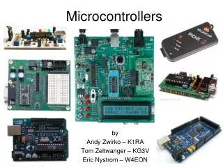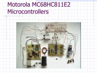
Motorola MC68HC811E2 Microcontrollers
640 likes | 903 Vues
Motorola MC68HC811E2 Microcontrollers. What will be covered within 3 classes. Class 1 Friday March 14 th (home work due Tuesday) What are Microcontrollers/Microprocessors Intro into the HC11 chip Registers, accumulators, Condition Code register, memory map and other components

Motorola MC68HC811E2 Microcontrollers
E N D
Presentation Transcript
What will be covered within 3 classes • Class 1 Friday March 14th(home work due Tuesday) • What are Microcontrollers/Microprocessors • Intro into the HC11 chip • Registers, accumulators, Condition Code register, memory map and other components • Class 2 Monday March 17th • Motorola Language Code • Data type and symbols • Opcodes, Operands and addressing modes • Class 3 (Tutorial) Tuesday March 18th • Assembler programming • Assembler Compiling • Assembler Emulating • All done using Oztech Electronics Software
Microprocessors • Microprocessors are components that compute binary mathematical commands at a specified rate determined by either an internal or external oscillating input. • Characterized by: • Memory addresses registers • Memory data registers • Instruction registers • Index registers • Stack registers • Accumulators • Program counters • Ex: Motorola Microprocessor 6800 (built in the 1980’s)
Microcontrollers • Microcontrollers are microprocessors that have built in peripherals, such as communications ports, I/O ports and others. These devices do not offer physical access to the address register and are usually standalone. They offer a fast and compact control method with limited physical connections and tools.
What they are used for • Remote monitoring equipment • Car computer systems • Automating equipment • Cell phones • Computers • Palm Pilots • Singing gift cards
HC11 • Power saving (stop) and (wait) modes • 2048 bytes of EEPROM • 256 bytes of RAM • 16 bit timer • 8-bit pulse accumulator • Real time interrupt circuit • Computer operating properly (COP) watchdog system
HC11 • Synchronous Serial Peripheral Interface (SPI) • Asynchronous Non return to Zero (NRZ) serial Communication Interface (SCI) • 8 channel, 8-bit analogue to digital (A/D) converters • 38 general purpose I/O pins • 16 bidirectional • 11 input only, 11 output only • Available in 52pin (PLCC) or 48 pin (DIP) packages
Nomenclature and symboles • Vdd and or Vss mean +5 volts. • GND = ground or 0 volts • PA1 means Port A pin 1 • Vrl = voltage reference low • Vrh = voltage reference high • Some pins have more than one function, these must be setup prior to use. Default is shown in manual. • Pins with a line above mean “not” or anti” polar. Thus when 0volts or a “low” is shown at the reset pin, the chip interprets as a 1 or a “high”.
Reset pin • All chips have a master reset pin where a physical reset can occur. • Used for emergencies • Low power • Frozen • Testing • Startup
Oscillator • All CPUs need an oscillator to jump between commands. • HC11 is a 4 cycle command chip • Operates at 2Mhz with an 8Mhz cristal
Interrupt Request Queue • There are many different interrupts on the HC11 • Software IRQ (SIR) • Multitude of input IRQ • Negative Edge Sensitive • Positive Edge Sensitive • Non-maskable IRQ (XIRQ) • Here nothing can stop the interrupt from occurring. • Always an external interrupt pin
Port A • Port A can be configured as: • Four timer input capture (IC) • Four timer output compare (OC) • Combination of the two • One pulse accumulator (PAI) • General I/O (note directional limits)
Port B • Port B can be configured for: • General purpose output pins • Simple Strobed output • Often used for 8-bit data communication
Port C • Port C pins can be configured for: • General I/O • Used for full handshake modes during parallel I/O • Often used as multiplexed address/data signal communication
Port D • Port D pins can be configured for: • General I/O • Serial Communication Interface (SCI) • Serial Peripheral Interface (SPI)
Port E • Port E pins can be configured for: • General purpose I/O • Analogue for digital input (A/D) • Note: for high accuracy of A/D, do not read port E during sampling of A/D, as small disturbances can reduce the accuracy of the results.
CPU Registers • HC11 has five registers and two accumulators • Accumulator D = accA + AccB to form a 16 bit accumulator
Condition Code Register (CCR) • C = Carry bit, ex: 255+1 = 0 + carry high • V = Overflow ex: 255+1 = 0 and v=1 as the sum has overflowed capacity • Z = zero bit ex: 1-1 = 0, z=1 • N = negative ex: 4-6 = $FD z=1 • I = interrupt mask, enables inturrupts • H = half carry (when carry is done from bit 3) • X = X interrupt mask XIRQ (set only by hardware (XIRQ and Reset pins), cleared only by software) • S = Stop disable (sleep mode mask)
Program Counter • The program counter always points to the next instruction location to be executed. • 16 bit register
Stack pointer • Stack is usually initialized at the top of memory and works down • The program is located at the bottom of memory and works up • If the stack grows too big, it may overwrite the program, causing a fatal crash • HC11 has 256 bytes of RAM for the stack • 16 bit register
Index Registers • HC11 has two index registers • X & Y are 16 bits wide • Used to index memory fetch or storage of large numbers
Accumulators • Accumulator A is 8 bits long • Accumulator B is 8 bits long • Accumulator D = A + B, where B is the low byte and A is the high byte. • AccD is used for large number handling • AccA and AccB are the main handlers of numbers within a program
Memory Map • 256 Bytes of RAM at top of memory address • 2K EEPROM from $F800 to $FFFF • 64 byte register block is mapped initially starting from $1000 (this includes mapped address for ports, pins and internal configuration setup) • All these can be remapped if needed
End of Day 1 • Assignment • Part1 • Given a input on the lower nibble (4 bit) of PortC, increment a counter by the input value. • Display counter output on PortB (8 bit) • Give a block diagram of events, decision and I/O • Part2 • Give a block diagram of a delay loop • Code the delay loop • Q: Calculate the time it takes to cycle through your delay loop. Hint: use a nested loop
Topics that will be covered • Motorola Language Code • Data type and symbols • Opcodes, Operands and addressing modes
Data types • The default numbering system is decimal in most compilers • Hexadecimal number are represented by a $ symbol. Ex: $FF = 255 decimal • A number is defined by a# ex1: #45 = 45 decimal. Ex2: #$45 = 69 decimal • Binary number are identified by a b. ex: #b101010 = #$2A = #42 decimal • Octave numbers are identified by an o ex: #o10 = #$9 = #9 decimal
Instruction Set (hand out in class) • Mnemonic = command • Operation = what it does • Description = description of how it does it • Addressing mode = the way it does it • Opcode = machine code that the HC11 sees • Cycles = number of cycles needed to compute • CCR = affected condition code after execution
Addressing modes • There are many ways of executing commands. • There are six different addressing modes • Immediate • Direct • Extended • Indexed • Inherent • relative
Immediate • Argument is contained in the byte(s) immediately following the opcode. • Number of bytes following the opcode matches the size of the register or memory location being operated on. • The effective address is the address of the byte following the instruction
Example of Immediate Source list: LDAA #$55 ‘load 55 hex into accA Object code: Memory location Memory contents 0100 86 0101 55
Inherent (accumulator/memory) • All information necessary to execute the instruction is contained in the opcode. • Operations that use only the index register or accumulators, as well as control instructions with no arguments, are included in this addressing mode. • These are one-byte or two-byte instructions
Example of Inherent Source list: PSHA ‘push accA to stack Object code: Memory location Memory contents 0100 36 Note: SP = SP -1
Direct addressing mode • The address is found in the next memory location following the opcode • This enables addressing the first page of memory (256 bytes) • Execution time is reduced due to less consumption of space and movement of bits
Example of direct Source list: LDAA $55 ‘load contents from address $0055 hex into accA Object code: Memory location Memory contents 0100 96 0101 55 … 0055 XX Note: After insturction, accA = XX
Indexed Addressing Mode • The offset, found in the second memory location of the instruction, is added to the contents of the index register to form a new effective address • The effective address is held in a temporary address register so that the contents of the index register are not changed
Example of Indexed Source list: ‘X=#$1000 LDAA #$55,X ‘load contents from address ($55 + X) hex into accA Object code: Memory location Memory contents 0100 A6 0101 55 … 1055 YY Note: After insturction, accA = YY
Extended Addressing mode • Used to address locations in full memory map • 2nd memory location = address high byte • 3rd memory location = address low byte
Example of Extended Source list: LDAA $2055 ‘load contents from address $2055 hex into accA Object code: Memory location Memory contents 0100 B6 0101 20 0110 55 … 2055 ZZ Note: After instruction, accA = ZZ
Relative Addressing Mode • Used for branch type instructions • Program control may be transferred to some place other than the next sequential memory location • Transfer is referenced from the next instruction which the MCU would execute if it did not transfer control • 2 byte instruction • 2nd byte contains the offset, which is the number of memory locations to branch over • Offset is expressed as an 8 bit 2’s compliment number
Example of Relative • Branch forward example Source list: BRA #$20 ‘branch forward 32 +1 positions Object code: Memory location Memory contents 0100 20 0101 20 0110 55 … 100100 RR 100101 DD Note: After branch, PC = 100110 and executing DD opcode Note2: Note that opcode for BRA = 20hex, and so is the jump. This is why a miscalculation of branching can crash your program
Example of Relative • Branch Backwards example Source list: BRA #$FE ‘branch backwards 2 - 1 positions Object code: Memory location Memory contents 0010 YY 0011 XX 0100 20 ‘BRA #$FE 0101 FE 0110 55 … 100100 RR 100101 DD Note: After branch, PC = 100 and executing 20 opcode Note2: Infinit loop
Subroutines • Branch to subroutine will push the PC onto the stack • This allows the program to return to the program once the subroutine has been executed. F800 BSRSUB FD00 SUB NOP FD01NOP FD02 RTS Memory map 00FF02 00FEF8