Download
1 / 51
530 likes | 920 Vues
Architecture of the C6x Processor. Zhu Ming / 朱明. Characteristics of C6x. The modified Harvard architecture von Neumann architecture Harvard pipeline Word length 32-bits, very-long instruction-word ( VLIW )architecture VELOCITI 1.2 C6713 & C6416

E N D
Architecture of the C6x Processor Zhu Ming / 朱明 EI
Characteristics of C6x • The modified Harvard architecture von Neumann architecture Harvard pipeline • Word length 32-bits, very-long instruction-word (VLIW )architecture • VELOCITI 1.2 • C6713 & C6416 C6713 floating-point, C6416 fixed-point “Explain the advantages and disadvantages of both the von Neumann architecture and the Harvard architecture, then expound their ties and differences.” EI
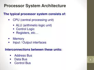
Diagram of one CPU’s architecture Bus is the circuit cables between the CPU and On-chip peripherals, such as memory. One circuit cable means one bit. The bus width is the number of bus cables. The bus width means the number of bit transmitted by bus at one time. So the number of circuit cables is the word length. For example, circuit cables of a chip are 8 means the word length of the chip is 8 bits or 1 byte, and the processing scale of the chip is byte, and its instruction is an 8-bits or 1-byte data. The circuit cables of C6416 DSP are 32 means the word length of our DSP is 32 bits or 1 word, and the processing scale of the chip is word, and the C6416’s instruction is a 32-bits or 1-word data. Byte is 8 bits, half-word are 16 bits, and word is 32 bits. 2014/9/14 3/45 EI
the implementation of an instruction Three stages: Program Fetch, Decode, Execute Implementation of an instruction is composed of three stages at least. Program Fetch means CPU read instruction from program memory. Decode means CPU analyze the instruction, analyze which is the instruction and analyze what will CPU do according to the instruction. ADD SUB MOV. Then CPU executes the instruction. 2014/9/14 4/45 EI
Keywords Von Neumann architecture (PPT) Harvard architecture (PPT) Harvard pipeline (PPT) modified Harvard architecture VLIW architecture VELOCITI architecture Pipeline of C6x 2014/9/14 5/45 EI
Von Neumann architecture • Three stages: Program Fetch, Decode, Execute • The von Neumann architecture is a serial architecture. PF>D>E>->-> PF>D>E >->-> PF>D>E (WYSIWYG) PC pointer points the instruction, means the previous instruction has been implemented completely, and the current instruction is ready to implement, but didn’t begin. PC pointer passes the instruction, means this instruction is being implemented. In von Neumann architecture, the outcomes of registers are consistent with PC pointer running. EI
Diagram of Von Neumann architecture • In Von Neumann architecture, there is only one bus in microprocessor. • So in one time, the CPU only can interface one memory. • Therefore, three stages of instruction, Program Fetch, Decode, and Execute, only can implement one stage at one time (not one cycle). Because of only one bus. EI
von Neumann architecture (PF>D>E>->-> PF>D>E >->-> PF>D>E) • Characteristic: serial architecture In von Neumann architecture, before the next instruction starts to implement, the previous instruction must has been implemented completely. • Advantage: easy for devices and designers • Von Neumann prediction every 18-months, size: half, speed: doubled • Disadvantage: resources waste EI
Keywords • von Neumann architecture • Harvard architecture • Harvard pipeline • modified Harvard architecture • VLIW architecture • VELOCITI architecture • Pipeline of C6x EI
the Harvard architecture Harvard pipeline (1) P Fetch> Decode > Execute (2) P Fetch > Decode >Execute (3) P Fetch > Decode >Execute • Comparing with von Neumann architecture, the Harvard architecture’s outcomes of registers are not consistent with PC pointer running. PC pointer running only means instruction programs fetch. The outcomes of instructions are decided by the stages of the Harvard pipeline. • So it is not WYSIWYG, What You See is not What You Get. EI
Diagram of Harvard architecture In the Harvard architecture the program bus and the data bus are separate. And program memory and data memory are separate. (1) P Fetch> Decode > Execute (2) P Fetch > Decode > Execute (3) P Fetch > Decode > Execute 2014/9/14 11/45 EI
the Harvard architecture (1) P Fetch> Decode > Execute (2) P Fetch > Decode > Execute (3) P Fetch > Decode > Execute • Characteristic: pipeline (so-call parallel) • Advantage: high-speed The Harvard architecture is a milestone in the ASIC field. • Disadvantages: complex & pipeline conflict =====NOP Comparing with von Neumann architecture, the Harvard architecture’s outcomes of registers are not consistent with PC pointer running. PC pointer running only means instruction program fetch. The outcomes of instructions are decided by the stages of the Harvard pipeline. EI
pipeline conflict & NOP • Factorial assembly n*(n-1)*(n-2)…3*2*1 .def _factfunc _factfunc: MV A4,A1 SUB A1,1,A1 LOOP: MPY A4,A1,A4 NOP SUB A1,1,A1 [A1] B LOOP NOP 5 B B3 NOP 5 .end
Homework “Explain the advantages and disadvantages of both the von Neumann architecture and the Harvard architecture, then expound their ties and differences.” 2014/9/14 14/45 EI
Keywords • von Neumann architecture • Harvard architecture • Harvard pipeline • modified Harvard architecture • VLIW architecture • VELOCITI architecture • Pipeline of C6x EI
Keywords • von Neumann architecture • Harvard architecture • Harvard pipeline • modified Harvard architecture • VLIW architecture • VELOCITI architecture • Pipeline of C6x EI
the great modified Harvard (3.4) • Several instructions within one pipeline (Program Fetch> Decode >Execute) MPY A7,B7,B6 ;multiply 16 LSBs of A7, B7 -> B6 || MPYH A7,B7,A6 ;multiply 16 MSBs of A7, B7 -> A6 • VLIW architecture very-long instruction-word • fetch packet (FP) one fetch packet can contain 8 instructions in C6x DSP • word length of C6x DSP is 256bits. EI
Keywords • von Neumann architecture • Harvard architecture • Harvard pipeline • modified Harvard architecture • VLIW architecture • VELOCITI architecture • Pipeline of C6x EI
Pipeline of C6x (3.5) 1. The program fetch stage is composed of four phases: (a) PG: program address generate (in the CPU) to fetch an address (b) PS: program address send (to memory) to send the address (c) PW: program address ready wait (memory read) to wait for data (d) PR: program fetch packet receive (at the CPU) to read opcode from memory 2. The decode stage is composed of two phases: (a) DP: to dispatch all the instructions within an FP to the appropriate functional units (b) DC: instruction decode EI
3. The execute stage is composed of 6 phases (with fixed point) to 10 phases (with floating point) due to delays (latencies) associated with the following instructions: (a) Multiply instruction, which consists of two phases due to one delay (b) Load instruction, which consists of five phases due to four delays (c) Branch instruction, which consists of six phases due to five delays LOOP: MPY A4,A1,A4 NOP SUB A1,1,A1 [A1] B LOOP NOP 5 Pipeline of C6x (3.5) EI
Pipeline of C6x (3.5) The functional unit latency (page 81) represents the number of cycles that an instruction ties up a functional unit. The latency is 1 for most instructions except double-precision instructions. Functional unit latency is different from a delay slot. For example, the instruction MPYDP has four functional unit latencies but nine delay slots. This implies that no other instruction can use the associated multiply functional unit for four cycles. A store has no delay slot but finishes its execution in the third execution phase of the pipeline. The NOPs equal to functional unit latency Most instructions have one execute phase. Instructions such as multiply (MPY), load (LDH/LDW), and branch (B) take two, five, and six phases, respectively. Additional execute phases are associated with floating-point and double-precision types of instructions, which can take up to 10 phases. EI
Keywords • von Neumann architecture • Harvard architecture • Harvard pipeline • modified Harvard architecture • VLIW architecture • VELOCITI architecture • Pipeline of C6x EI
FETCH AND EXECUTE PACKETS (3.4) • Fetch Packet (FP) • Execute Packet (EP) EP (instructions) FP EP (instructions) EP (instructions) • VELOCITI architecture EI
Pipelining Effects (3.20.4) • Pipelining Effects with More Than One EP within an FP EI
Architecture of C6x • Architecture of CPU (3.2) • Buses and Memory • Memory and .CMD file • Functional units • Registers • Timers • McBSPs • DMA EI
Architecture of C6713 • C6713 has two sets of register files, each set with 16 registers. • Internal memory includes a two-level cache architecture with 4 kB of level 1 program cache (L1P), 4 kB of level 1 data cache (L1D), and 256 kB of level 2 memory shared between program and data space. It has a direct interface to both synchronous memories (such as SDRAM and SBSRAM) and asynchronous memories (such as SRAM and EPROM). Synchronous memory requires clocking but provides a compromise between static SRAM and dynamic DRAM, with SRAM being faster but more expensive than DRAM. • On-chip peripherals include two McBSPs (multichannel buffered serial ports), two timers, a host port interface (HPI), and a 32-bit EMIF the external memory interface. • C6713 DSP requires 3.3 Voltage for I/O pins and 1.26 Voltage for the core (internal). 3.3 Voltage is general I/O voltage. But the different DSP require different core voltage. EI
Architecture of C6x • Architecture of CPU • Buses and Memory • Memory and .CMD file • Functional units • Registers • Timers • McBSPs • DMA EI
Internal Buses of C6x (3.2) • Internal buses include a 32-bit program address bus, a 256-bit program data bus to accommodate eight 32-bit instructions, two 32-bit data address buses, two 64-bit data buses, and two 64-bit store data buses. With a 32-bit address bus, the total memory space is 232 = 4GB, including four external memory spaces: CE0, CE1, CE2, and CE3. • Notes: these buses maybe only access one memory, one multi-interface memory. EI
Typical linker command file of C6x (1.7.3) • /*C6416dsk.cmd Linker command file*/ • MEMORY • { • IVECS: org=0h, len=0x220 • IRAM: org=0x00000220, len=0x0002FDE0 /*internal memory*/ • SDRAM: org=0x80000000, len=0x00100000 /*external memory*/ • FLASH: org=0x90000000, len=0x00020000 /*flash memory*/ • } • SECTIONS • { • .EXT_RAM :> SDRAM • .vectors :> IVECS /*in vector file*/ • .text :> IRAM /*Created by C Compiler*/ • .bss :> IRAM • .cinit :> IRAM • .stack :> IRAM • .sysmem :> IRAM • .const :> IRAM • .switch :> IRAM • .far :> IRAM • .cio :> IRAM • .csldata :> IRAM • } EI
Architecture of C6x • Architecture of CPU • Buses and Memory • Memory and .CMD file • Functional units • Registers • Timers • McBSPs • DMA EI
Internal L2 memory of C6x (3.2) C6713 C6416 EI
Typical linker command file of C6x (1.7.3) • /*C6416dsk.cmd Linker command file*/ • MEMORY • { • IVECS: org=0h, len=0x220 • IRAM: org=0x00000220, len=0x0002FDE0 /*internal memory*/ • SDRAM: org=0x80000000, len=0x00100000 /*external memory*/ • FLASH: org=0x90000000, len=0x00020000 /*flash memory*/ • } • SECTIONS • { • .EXT_RAM :> SDRAM • .vectors :> IVECS /*in vector file*/ • .text :> IRAM /*Created by C Compiler*/ • .bss :> IRAM • .cinit :> IRAM • .stack :> IRAM • .sysmem :> IRAM • .const :> IRAM • .switch :> IRAM • .far :> IRAM • .cio :> IRAM • .csldata :> IRAM • } EI
memory on C6416 experiment board • Programs and data are within internal L2 memory. • External SDRAM generally is used to save the large data file, such as speech data file. In chapter 2, there is an example (the second last) to use external SDRAM to save your speech data. • External Flash also can be used to save the large data file, and can be used to save the DSP programs. In our experiment, we use PC download the programs to DSP. But for DSP product, programs are saved in Flash. When DSP product is turned on, DSP first loads the programs in Flash to internal memory, then loads the instructions from internal memory to CPU one by one. The last example in chapter 2 is about changing and downloading the programs to Flash on our experiment board. EI
Independent memory banks (3.2) Independent memory banks on the C6x allow for two memory accesses within one instruction cycle. No conflict results if the data accessed are in different memory banks. Separate buses for program, data, and direct memory access (DMA) allow the C6x to perform concurrent program fetches, data read and write, and DMA operations. Data and instructions reside in separate memory spaces Internal memory is organized as separate program and data memory spaces, with two 32-bit internal ports (two 64-bit ports with the C64x) to access internal memory. The C6x has a byte-addressable memory space. The extra registers of C64x allow for packed data types to support four 8-bit or two 16-bit operations associated with one 32-bit register. MPYU4 Several special-purpose instructions have also been added to handle many operations encountered in wireless and digital imaging applications, where 8-bit data processing is common. 2014/9/14 40/45 EI
Architecture of C6x • Architecture of CPU • Buses and Memory • Memory and .CMD file • Functional units • Registers • Timers • McBSPs • DMA EI
FUNCTIONAL UNITS (3.3) • eight independent functional units divided into two data paths, A and B. • multiply operations (.M) • logical and arithmetic operations (.L) ALUs • branch, bit manipulation, and arithmetic operations (.S) ALUs • loading/storing and arithmetic operations (.D) ALUs • The .S and .L units are for arithmetic, logical, and branch instructions. All data transfers make use of the .D units. • In addition, the .M unit of C64x DSP can also handle shift and rotate operations, the .D unit can also handle logical operations. • The arithmetic operations, such as subtract or add (SUB or ADD), can be performed by all the units, except the .M units (one from each data path). • The eight functional units consist of four floating/fixed-point logical and arithmetic units ALUs (two .L and two .S), two fixed-point ALUs (.D units), and two floating/fixed-point multipliers (.M units). EI
Dispatch functional units (3.3) If you want to get the most effective assembler, you must dispatch the functional units in the instruction codes by yourselves. Sometimes, if you use the ill-suited functional units in the instructions, your program will become no effective, and even illegal. If you want to get the programs fast, you may ignore the functional units in the instruction codes, and CCS complier will dispatch the functional units. Of course the programs may be not the most effective, but must be correct. .def _sumfunc _sumfunc: MV .L1 A4,A1 SUB .S1 A1,1,A1 LOOP: ADD .L1 A4,A1,A4 SUB .S1 A1,1,A1 [A1] B .S2 LOOP NOP 5 B .S2 B3 NOP 5 .end .def _sumfunc _sumfunc: MV A4,A1 SUB A1,1,A1 LOOP: ADD A4,A1,A4 SUB A1,1,A1 [A1] B LOOP NOP 5 B B3 NOP 5 .end 2014/9/14 43/45 EI
FUNCTIONAL UNITS (3.3) • Each functional unit can read directly from or write directly to the register file within its own path. Each path includes a set of sixteen 32-bit registers, A0 through A15 and B0 through B15. C64x DSP has 32 32-bit registers, A0 through A31 and B0 through B31. • Units ending in 1 write to register file A, and units ending in 2 write to register file B. • Two cross-paths (1x and 2x) allow functional units from one data path to access a 32-bit operand from the register file on the opposite side. There can be a maximum of two cross-path source reads per cycle. • Each functional unit side can access data from the registers on the opposite side using a cross-path. • There are 32 general purpose registers, but some of them are reserved for specific addressing or are used for conditional instructions. All data processed by C6x DSP are in these registers. EI
REGISTERS (3.6) • A0, A1, B0, B1, B2: conditional registers • A4…A7, B4…B7: circular addressing • A0…A9, B0…B9 (except B3): temporary registers • B3: current PC pointer save register, for interrupt or subroutine returning. • A4, B4, A6, B6, A8, B8, A10, and B10 are used to transfer parameters between main and sub routine. • A10…A15, B10…B15 : saved & later restored • A 40-bit data value can be contained across a register pair. The 32 least significant bits (LSBs) are stored in the even register (e.g., A2), and the remaining 8 bits are stored in the 8 LSBs of the next-upper odd register (A3). A similar scheme is used to hold a 64-bit double-precision value within a pair of registers (even and odd). • The C64x can read or write 128 bits per cycle EI
TIMERS (3.13) • Two or three 32-bit timers can be used to time and count events or to interrupt the CPU. A timer can direct an external ADC to start conversion or the DMA controller to start a data transfer. A timer includes a time period register, which specifies the timer’s frequency; a timer counter register, which contains the value of the incrementing counter; and a timer control register, which monitors the timer’s status. • In our experiment, we use a timer to control the sampling frequency of ADC and DAC. EI
Memory Map Summary of C6416T (3.2) …… 2014/9/14 47/45 EI
MULTICHANNEL BUFFERED SERIAL PORTS (3.15) • Two or three McBSPs are available on C6x. • McBSPs provide an interface to inexpensive (industry standard) external peripherals. McBSPs have features such as full-duplex communication, independent clocking and framing for receiving and transmitting, and direct interface to SPI, IIC and IIS compliant devices. • McBSPs of C6x allow several data sizes between 8, 16, 24 and 32 bits. EI
Internal block diagram of McBSP (3.15) • data transmit (DX) data receive (DR) pins • CLKX, CLKR, FSX, FSR • data receive register (DRR) data transmit register (DXR) • transmit shift register (XSR) receive shift register (RSR) • receive buffer register (RBR) • The two McBSPs are used for input and output on our experiment system. McBSP0 is used for control and McBSP1 for transmitting and receiving data. EI
DIRECT MEMORY ACCESS (3.16) • DMA allows for the transfer of data to and from internal memory or external devices without intervention from the CPU. 16 enhanced DMA channels (EDMA) can be configured independently for data transfer. • DMA can access on-chip memory and the EMIF, as well as the HPI. • Data of different sizes can be transferred: 8-bit bytes, 16-bit half-words, and 32-bit words. • Address (source and destination), index, count reload, DMA global data, and control registers. • DMA transfers can be triggered by interrupts from internal peripherals as well as from external pins • Each DMA channel can be programmed for priorities with the CPU. Each DMA channel can be made to start initiating block transfer of data independently. • A block can contain a number of frames. Within each frame can be many elements. Each element is a single data value. EI