Processor Design Specifying the Actions Internal Architecture of a Simple Processor
350 likes | 590 Vues
Processor Design Specifying the Actions Internal Architecture of a Simple Processor. ITCS 3181 Logic and Computer Systems 2014 B. Wilkinson Slides6.ppt Modification date: March 27, 2014. Internal Architecture of a Simple Processor

Processor Design Specifying the Actions Internal Architecture of a Simple Processor
E N D
Presentation Transcript
Processor Design Specifying the Actions Internal Architecture of a Simple Processor ITCS 3181 Logic and Computer Systems 2014 B. Wilkinson Slides6.ppt Modification date: March 27, 2014
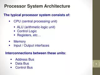
Internal Architecture of a Simple Processor (Not representative of modern computer, later on that)
MDR and MAR registers Added to hold data or from memory and address to select memory location:
Internal Operation • Operation of processor divided into two phases: • Fetch cycle • Next instruction is fetched from memory • Execute cycle • Fetched instruction is executed • These cycles are repeated as each instruction is executed.
Fetch Cycle Select instruction:
Register Transfer Notation Mostly, actions within processor can be described by the transfer of the contents of one location to another location (registers or units). Use a register transfer language (RTL) notation. Example To transfer the contents of register MDR to register IR, we write: IR MDR
May add time of action: T2: IR MDR The transfer is to take place at time period T2.
Fetch Cycle Fetch cycle actually breaks down into several steps: T0: MAR PC Select next instruction T1: MDR [MAR] Memory read operation, get instr. from memory T2: IR MDR Load instruction into instruction register T3: PC PC + 4 Increment program counter in preparation for next fetch cycle Could be done simultaneously
Fetch Cycle Fetch cycle with last two steps done simultaneously: T0: MAR PC Select next instruction T1: MDR [MAR] Mem. read op., get instr. from mem. T2: IR MDR; PC PC + 4 Load instruction into instr. register Increment prog. counter in prep. for next fetch cycle
Execute Cycle Breaks down into several steps depending upon instruction fetched. In our design, execution cycle steps start at T3. To be able to specify certain steps, need to know machine instruction format. We will give representative formats, which will be used in subsequent designs later.
Source and destination registers We will use the notation: Rs1 for the first source register Rs2 for the second source register Rd for the destination register for register-register instructions as specified in the instruction. Some instructions may only have one source register and/or no destination register.
Temporary registers In some designs, it may be necessary to introduce temporary registers to hold Rs1, Rs2, Rd, say called A, B, and C. Then: A Rs1 Contents of first source register copied to A B Rs2 Contents of second source register copied to B will occur automatically whether or not they required by the instruction. If not required, A and B are not accessed subsequently. Similarly if C is loaded, the operation: Rd C Copy C to destination register occurs automatically.
Execute Cycle for Add Instruction Register-register addressing Example: ADD Rd, Rs1, Rs2 T3: Rd Rs1 + Rs2 Perform addition and pass result back to Rd
Execute Cycle for Add Instruction Immediate Addressing ADDI Rd, Rs1, 123 T3: Rd Rs1 + IR15-0 Perform addition and pass result back to Rd IR15-0 means here bits 15 to 0 of IR register Assumes bits 15 to 0 in IR holds the constant (123 above)
Other Arithmetic/Logic Instructions Other arithmetic and logic instructions have similar sequences of steps. Simply replace the add operation in: T3: Rd Rs1 + Rs2 Perform addition and pass result back to Rd or T3: Rd Rs1 + IR15-0 Perform addition and pass result back to Rd with the appropriate arithmetic or logic operation.
Execute Cycle for Memory Reference Instructions Load Instruction LD Rd, 100[Rs1] where 100 is a constant in the instruction (IR15-0) T3: MAR Rs1 + IR15-0 Compute memory address T4: MDR [MAR] Memory read operation T5: Rd MDR Get memory contents, load into Rd
Store Instruction ST 100[Rs1], Rs2 where 100 is a constant in the instruction (IR15-0) T3: MAR Rs1 + IR15-0 Compute memory address T4: MDR Rs2 Get contents of register T5: [MAR] MDR Memory write operation
Branch Instructions Bcond Rs1, L1 where cond specifies the condition, E, NE, L, G, GE, or LE. T3: Rs1 - 0 Compare Rs1 with zero T4: if (condition TRUE) PC PC + IR15-0 Load PC with target address Offset stored in instruction needs to be offset – 4 since PC already incremented by 4 by this time. Also need to take into account the offset is a word offset - not shown here.
Jump Instruction PC-Relative Addressing J L1 T3: PC PC + IR25-0 Load PC with target address Again offset stored in instruction needs to be offset - 4
Jump Instruction Register-Indirect Addressing J 100[Rs1] where the offset (100 above) is held in IR15-0 T3: PC Rs1 + IR15-0 Compute effective address and load PC with final target address
Jump and Link Instruction JAL L1 T3: R31 PC Store return address in R31 T4: PC PC + IR25-0 Goto L1
CALL/RET Instructions Even though our design does not have CALL and RET instructions, let us just list the steps for these instructions: CALL proc1 T3: SP SP – 4Decrement stack pointer (by 4 if 32-bit addresses) T4: MAR SP T5: MDR PC PC holds return address T6: [MAR] MDR Copy PC onto stack (return address) T7: PC IR25-0 Gototo procedure (address of proc1 held in IR25-0) RET T3: MAR SP T4: MDR [MAR] Get return address from stack T5: PC MDR Return T6: SP SP + 4 Increment stack pointer (by 4 if 32-bit addresses)
Register-Register Instructions The arithmetic and logic instructions operating upon pairs of registers - Could be many such instructions. For simplicity, let us assume the following six operations: ADD Addition SUB Subtract MULT Multiply DIV Divide AND Logical AND OR Logical OR
State diagram for register-register instructions All very similar form: MUL/DIV almost certain to require more that one cycle but this is ignored here.
Register-Constant Instructions The arithmetic and logic instructions operating upon one register and an immediate constant For simplicity, let us assume the following six operations: ADDI Addition SUBI Subtract ANDI Logical AND ORI Logical OR SHL Logical shift left (number of places given by constant) SLR Logical shift right (number of places given by constant) The “I” is used here to indicate immediate addressing.
State diagram for register-constant instructions All very similar form:
Conditional Branch Instructions Let us assume the conditional branch instruction of the format: Bcond, Rs1, L1 (not using a CCR) and the following four operations: BL Branch if Rs1 less than zero BG Branch if Rs1 greater than zero BE Branch if Rs1 equal zero BNE Branch if Rs1 not equal zero Question – is that sufficient?
Execute Cycle for Branch Instruction • In this case we need to select on of two sets of actions: • If branch condition true = do actions (alter PC) • If branch condition false, generally do nothing.
State Diagram of Branch Instructions All of similar format:
Could combine states 22, 24, 26, and 28 into one state, and combine states 29 and 32 into one state. However in our design will only combine 29 and 32 to get 32 states in total (0 to 31):
Questions Next step is to implement state diagrams.