Download

1 / 16
160 likes | 180 Vues
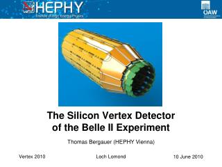
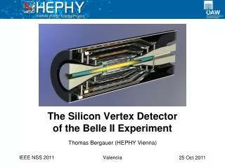
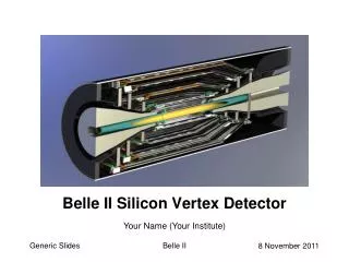
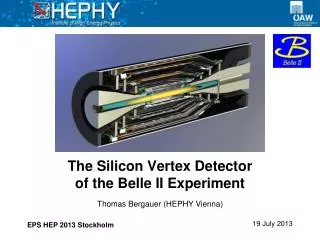
Striplet option of Super Belle Silicon Vertex Detector. Talk at Joint Super B factory workshop, Honolulu 20 April 2005 T.Tsuboyama. Super B Silicon Vertex Detector. Idea is already given in LoI (2004) assuming a luminosity of 2.5x10 35 /cm 2 /sec. Points of upgrade is

E N D
Striplet option of Super BelleSilicon Vertex Detector • Talk at • Joint Super B factory workshop, Honolulu • 20 April 2005 • T.Tsuboyama
Super B Silicon Vertex Detector • Idea is already given in LoI (2004) assuming a luminosity of 2.5x1035/cm2/sec. • Points of upgrade is • Immunity to background is realized by VA1TA readout. • Striplet sensor for the inner most layer. • R=1 cm chamber and R=1.3 cm for the 1st layer. • Better vertex resolution is necessary in order to reject non B-Bbar events in rare B decay analyses. • Coverage • Angular acceptance: 15 < θ < 150˚ (same as for SVD2)
Geometry • Angular acceptance: 15 < θ < 150˚ (same as for SVD2). • Radius 1.3 cm < R < 14 cm (1.5< R < 10 cm for SVD2) • First layer is at 1.3 cm: Better impact parameter resolution. • CDC can not be operated at R<14 cm. SVD2
Reduction of occupancy • The BKG hit rate in the 1st layer amounts to 20-30 times than now. (O.Tajima) • BKG (occupancy) should be reduced at least 1/30 in order to keep the tracking quality. • Sensitive time (shaping time) to 1/8 • Active area per strip to 1/6 • Readout with APV25 chip. (SVD2: VA1TA) • 50 nsec shaping (SVD2 ➔ 800 nsec) • Further background reduction possible (M.Pernicka) • Striplet sensor • Strip area: 0.42 mm2 (SVD2). 0.06 mm2. (SuperB) • Pixel option: ultimate solution (G. Varner)
Striplet DSSD • Sensitive area of L1 DSSD • With 50 μm pitch readout, we can make 170 strips in r-Φ direction and 1420 strips in z-side. • Kapton flex cable is used to read out z-side strips. • Striplet sensor • Put strips at 45°With 50 μm pitch readout, we can make 1024 strips on both sides. • Read out using high density Kapton flex cable on both sides. 8.5 mm 71.0 mm
Striplet configuration • Strip is arranged at 45 degrees on both sides. • There is an insesitive region at each corner (3.5 %)
Cons and Pros • Cons • Insensitive region at each corner (7% in case of Super Bell layer 1 DSSD) • R-Φ and Z coordinates are calculated from U and V measurement. • Reconstruction and simulation software become complicated. • Measurements in R-Φ and Z measurement fully correlate. • Pros • Strip configuration on P-side and N-side is automatically determined independent of the length/width ratio. • Same number of readout on p-side and n-side. • Spatial resolution, cluster size of R-Φ and Z is always similar. • Rooms to improvement without much pain/cost.
Evaluation of Test sensor • Test production was done in HPK in 2003 • Laser scan test was done in KEK with VA1TA. • Test with APV25 readout was done in CERN and KEK beam line (M.Pernicka)
Laser scan • Charge collection efficiency between n-side and p-side was measured with semiconductor pulse laser: λ=845 nm, spot size<10 μm. • When position dependence in p-side is measured, the laser was injected from n-side and moved parallel to n-side strips, vice versa. • Charge collection efficiency in central region (①) and around the triangle region (②) was measured. ② ①
Laser scan result (I) • Central region. • Charges measured in the scan side is divided by total charge in the injection side. • Both n-side and p-side data show good charge sharing curve. • No indication of charge loss.
Laser scan result (II) • Here, laser scan was done close to triangle region. • P-side strips only: Scan in n-side can not be done due to mechanical problem for the wire bonding. • Total charge is flat above the second strip. • Total charge decreased to 80 % at the first strip. • Charge in the 1st strip is same. • Loss is consistent with charge escaped to the triangle region.
Improvement of strip pattern • Avoid insensitive region • Variable angle to fill the whole space with strips. (D. Heffernan) • In order to keep the minimum distance between strips, the strip spacing in • is wider than 100 μm.-->Anothe design.
Strip pattern improvement(II) • Put strips in the wide strip-gap region. • Maximum strip-gap becomes 100 um.
Cluster size in forward region. • In the forward region, track passes DSSDs with shallow angle, resulting many strips hits. • Cluster finding efficiency decreases. • Narrow cluster pitch does not contribute to spatial resolution because of large charge fluctuation. • Optimization of strip pitch will be necessary based on beam test and Monte Carlo simulation.
Summary • Based on LoI proposal, a striplet sensor for the SVD Layer 1 is produced. • Charge collection efficiency was checked with laser scan system. • Uniform charge collection efficiency was confirmed. • Design of striplet sensor is improving taking the laser scan, test beam result into consideration. • Monte Carlo simulation is necessary in order to finalize the detail design. • Schedule
2005 2006 2007 2008 2009 2010 2011 Luminosity (1034) 2.0 3.0 5.0 5.0 0 0 25 SVD2.0 Reinforcement SVD2.0→SVD2.5 Replace L1 ladders SVD2.5→SVD3 Full upgrade Upgrade schedule • Layer 1 replacement is scheduled in 2007 summer • SVD3 schedule depends on approval of the project. Test R&D Prod. Test R&D Installation Prod.