Download
1 / 8
80 likes | 110 Vues
Contemporary eld programmable gate array FPGA design requires a spectrum of available physical resources. As FPGA logic capacity has grown, locally accessed FPGA embedded memory blocks have increased in importance. When targeting FPGAs, application designers often specify high level memory functions, which exhibit a range of sizes and control structures. These logical memories must be mapped to FPGA embedded memory resources such that physical design objectives are met. In this paper, a set of power efficient logical to physical RAM mapping algorithms is described, which converts user de ned memory speci cations to on chip FPGA memory block resources. These algorithms minimize RAM dynamic power by evaluating a range of possible embedded memory block mappings and selecting the most power ef cient choice. Our automated approach has been validated with both simulation of power dissipation and measurements of power dissipation on FPGA hardware. A comparison of measured power reductions to values determined via simulation con rms the accuracy of our simulation approach. Our power aware RAM mapping algorithms have been integrated into a commercial FPGA compiler and tested with 34 large FPGA benchmarks. Through experimentation, we show that, on average, embedded memory dynamic power can be reduced by 26 and overall core dynamic power can be reduced by 6 with a minimal loss 1 in design performance. In addition, it is shown that the availability of multiple embedded memory block sizes in an FPGA reduces embedded memory dynamic power by an additional 9.6 by giving more choices to the computer aided design algorithms. Bhagyashree Ashok Gavhane | Prashant Vitthalrao Kathole "Alternative RAM Mapping Algorithm for Embedded Memory Blocks in FPGA" Published in International Journal of Trend in Scientific Research and Development (ijtsrd), ISSN: 2456-6470, Volume-2 | Issue-3 , April 2018, URL: https://www.ijtsrd.com/papers/ijtsrd7172.pdf Paper URL: http://www.ijtsrd.com/engineering/electronics-and-communication-engineering/7172/alternative-ram-mapping-algorithm-for-embedded-memory-blocks-in-fpga/bhagyashree-ashok-gavhane<br>

E N D
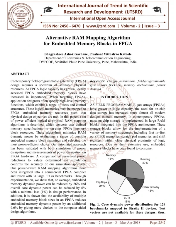
International Research Research and Development (IJTSRD) International Open Access Journal Alternative RAM Mapping Algorithm for Embedded Memory Blocks in FPGA for Embedded Memory Blocks in FPGA International Journal of Trend in Scientific Scientific (IJTSRD) International Open Access Journal ISSN No: 2456 ISSN No: 2456 - 6470 | www.ijtsrd.com | Volume 6470 | www.ijtsrd.com | Volume - 2 | Issue – 3 Alternative RAM Mapping Algorithm for Embedded Memory Blocks in FPGA Bhagyashree Ashok Gavhane Department of Electronics & DYPCOE, Savitribai Phule Pune University, Pune, Maharashtra, ibai Phule Pune University, Pune, Maharashtra, India Bhagyashree Ashok Gavhane, Prashant Vitthalrao Kathole Department of Electronics & Telecommunication Engineering, Prashant Vitthalrao Kathole India ABSTRACT Contemporary field-programmable gate array (FPGA) design requires a spectrum of available physical resources. As FPGA logic capacity has grown, locally accessed FPGA embedded memory blocks have increased in importance. When targeting FPGAs, application designers often specify high- functions, which exhibit a range of sizes and control structures. These logical memories must be mapped to FPGA embedded memory resources such that physical design objectives are met. In this paper, a set of power efficient logical-to-physical RAM mapping algorithms is described, which converts user memory specifications to on-chip FPGA memory block resources. These algorithms minimize RAM dynamic power by evaluating a range of possible embedded memory block mappings and selecting the most power-efficient choice. Our automated approach has been validated with both simulation of power dissipation and measurements of power dissipation on FPGA hardware. A comparison of measured power reductions to values determined via simulation confirms the accuracy of our simulation approach. Our power-aware RAM mapping algorithm been integrated into a commercial FPGA compiler and tested with 34 large FPGA benchmarks. Through experimentation, we show that, on average, embedded memory dynamic power can be reduced by 26% and overall core dynamic power can be reduced by 6% with a minimal loss (1%) in design performance. In addition, it is shown that the availability of multiple embedded memory block sizes in an FPGA reduces embedded memory dynamic power by an additional 9.6% by giving more choices to the computer design algorithms. programmable gate array (FPGA) Keywords: Design automation, gate arrays (FPGAs), memory architecture, power demand I. INTRODUCTION AS FIELD-PROGRAMMABLE gate arrays (FPGAs) have grown in logic capacity, the need for on data storage has increased since designs contain memory. In contemporary FPGAs, most on-chip storage is implemented in large RAM blocks integrated into the FPGA architecture. These storage blocks allow for the implementation of a variety of memory structures, including out (FIFO) memories, scratch pad memories, and shift registers, within close physical proximity of logic resources. Due to their extensive use, embedded memory blocks have been found to consume Design automation, field-programmable mory architecture, power design requires a spectrum of available physical resources. As FPGA logic capacity has grown, locally accessed FPGA embedded memory blocks have increased in importance. When targeting FPGAs, -level memory functions, which exhibit a range of sizes and control ures. These logical memories must be mapped to FPGA embedded memory resources such that PROGRAMMABLE gate arrays (FPGAs) have grown in logic capacity, the need for on-chip has increased since almost all modern designs contain memory. In contemporary FPGAs, chip storage is implemented in large RAM blocks integrated into the FPGA architecture. These storage blocks allow for the implementation of a variety of memory structures, including first in–first ories, scratch pad memories, and shift registers, within close physical proximity of logic resources. Due to their extensive use, embedded memory blocks have been found to consume. . In this paper, a set physical RAM mapping described, which converts user defined chip FPGA memory block resources. These algorithms minimize RAM dynamic power by evaluating a range of possible embedded memory block mappings and selecting the ficient choice. Our automated approach oth simulation of power dissipation and measurements of power dissipation on FPGA hardware. A comparison of measured power reductions to values determined via simulation firms the accuracy of our simulation approach. aware RAM mapping algorithms have been integrated into a commercial FPGA compiler and tested with 34 large FPGA benchmarks. Through experimentation, we show that, on average, embedded memory dynamic power can be reduced by 26% and overall core dynamic power can be reduced by 6% a minimal loss (1%) in design performance. In addition, it is shown that the availability of multiple embedded memory block sizes in an FPGA reduces embedded memory dynamic power by an additional 9.6% by giving more choices to the computer-aided Fig. 1.Core dynamic power distribution for 124 benchmarks mapped to Stratix II devices. Test vectors are not available for these designs; thus, vectors are not available for these designs; thus, Core dynamic power distribution for 124 benchmarks mapped to Stratix II devices. Test @ IJTSRD | Available Online @ www.ijtsrd.com @ IJTSRD | Available Online @ www.ijtsrd.com | Volume – 2 | Issue – 3 | Mar-Apr 2018 Apr 2018 Page: 2542
International Journal of Trend in Scientific Research and Development (IJTSRD) ISSN: 2456-6470 implementation and selects the most power-efficient implementation subject to on-chip RAM availability constraints. When necessary, userspecified RAM control signals (R/W enable and clock enables) are remapped to achieve a logically equivalent RAM implementation with reduced consumption. If an FPGA contains embedded memory blocks of different sizes, a mapping using each block type is considered. Our mapping techniques have been integrated into the Altera Quartus II synthesis system [1] and targeted to several Altera FPGA families, which contain embedded memories. To determine the benefit of our approach, we evaluate the power reduction for 34 designs, which contain RAM using a power estimation methodology based on digital simulation and circuit level power models. To evaluate the accuracy of the simulation based approach, we first map a sample set of six large FPGA designs and a group of primitive RAM instantiations to an FPGA-based board, which allows for accurate dynamic power measurements. Through experimentation with the sample designs, it is shown that the measured and predicted power savings due to our mapping optimizations differ by a little more than one percentage point. Subsequent simulation-based experimentation with the 34 RAM- based designs demonstrates an average embedded memory dynamic power reduction of 26% and overall core dynamic power reduction of 6% on Stratix II devices. In addition, the availability of multiple types of embedded memory blocks in an FPGA device reduces memory dynamic power and overall core dynamic power by an additional 9.6% and 2%, respectively. In the next section, we discuss related power-aware memory mapping techniques. In Section III, the basic operation of FPGA embedded memories is described along with details of the basic mapping flow used to translate user-specified logical memory to physical embedded memory blocks. Section IV provides the details of our power-aware RAM mapping techniques and supporting algorithms. Experimental results are presented in Section V. Section VI summarizes the paper and provides directions for future work. II. RELATED WORK RAM dynamic power-reduction techniques for application specified integrated circuits (ASICs) and microprocessor systems have been considered at the application mapping, compiler, and circuit levels. Although these approaches provide insight into logic is assumed to toggle during 12.5% of clock cycles. between 10% and 20% of core dynamic power in typical FPGA designs [1]. For example, Fig. 1 illustrates the core dynamic power breakdown for 124 FPGA designs of varying sizes and functionalities mapped to Altera Stratix II [2] devices. On average, embedded memory consumes as much power as lookup tables (LUTs) in these designs. As the amount of FPGA logic and on-chip memory increases over the next few years and the application domain of FPGAs expands to include mobile and power- sensitive environments, the power-efficient use of embedded memory blocks will become increasingly important. Embedded contemporary FPGAs are typically implemented with synchronous static RAM (SRAM) [2], [19] to improve design performance. Like other synchronous SRAM architectures, FPGA embedded memory accesses are performed in concert with a design clock and a series of interface signals including read/write (R/W) enables, clock enables, address, and data signals. During application development, designers usually do not specify RAM blocks that precisely match the size and fully specify the control signals of the physical RAM blocks on an FPGA. More typically, a higher level representation is specified, and the computer-aided design (CAD) flow automatically implements this specification using “physical memories” and any required control circuitry. Synchronous FPGA embedded memories primarily consume dynamic power as a result of internal RAM clocking. To save power, RAM control signals can be configured to suppress internal clocking when RAM access is unnecessary on a specific clock cycle. Although user- defined or generated control signals provide for valid functional embedded memory behaviour, their configuration may not unnecessary clocked memory accesses, leading to wasted RAM dynamic power. These limitations motivate the development of RAM mapping algorithms that take power objectives into account while maintaining valid functional behaviour. In this paper, we describe a series of algorithms to automatically map user-specified logical memories to available physical embedded memory block resources with the goal of reducing overall FPGA dynamic power consumption. In considering feasible RAM mappings, our approach estimates the relative dynamic power consumption of each potential dynamic power memory blocks in “logical memory” efficiently suppress @ IJTSRD | Available Online @ www.ijtsrd.com | Volume – 2 | Issue – 3 | Mar-Apr 2018 Page: 2543
International Journal of Trend in Scientific Research and Development (IJTSRD) ISSN: 2456-6470 reducing FPGA embedded memory power, none are directly applicable. Several synthesis techniques for application-specific embedded systems create power- optimized memory structures based on application address traces. In [5], the memory trace of an embedded application is analyzed by an algorithm to determine the portion of program and data memory that is most frequently accessed. These addresses are then grouped into memory banks, which are implemented with scratch pad memories. Infrequently accessed addresses are grouped into larger physical memory blocks. Later work by Cao et al. [6] extends this optimization to consider data width scaling. Wuytack et al. [18] have developed techniques to optimize the entire memory hierarchy of an application for power consumption based on application information. These previous approaches rely on application trace information to perform memory partitioning. A number of compiler techniques have been developed for processor-based systems, which optimize power while mapping data to fixed system memory resources. For example, in [16], a series of memory locations for multimedia applications are remapped to a small local scratch pad memory to save dynamic power. In [13], the organization and power consumption of a translation look-aside buffer are adjusted on a per-application basis. In [8], memory energy is managed through memory and register allocation using a network flow algorithm. In [7], a compiler technique to optimize sleep-mode operation for memories is described. Memory reactivations are minimized via scheduling to save dynamic power. Numerous circuit-level techniques for power reduction have been explored [11] including reduced swing pre-decode lines, multistage address decoding, and divided word and bit lines, among others. These techniques may be used in the future by FPGA designers to reduce FPGA embedded memory block power and are additive to the approaches described in this paper. Although FPGA logic and routing dynamic power reduction has been studied [10], these techniques were not applied to embedded memory blocks. Except for [15], previous research efforts that map design logic to embedded memory blocks in ASICs [4], [14] and FPGAs [9] do not consider power optimization as a mapping goal. This paper extends our earlier work in [15] by providing more descriptions and many new experimental results. We validate our simulation-based power estimation approach by comparing the power reductions estimated via simulation with those measured on physical hardware for a subset of our design suite and show that the results are very consistent. We also measure all power reductions due to our RAM mapping algorithm using a more recent version of the Quartus CAD tool than the one used in [15]. This more recent version of the Quartus software includes synthesis, placement, and routing algorithms, which incorporate power optimizations; thus, the results in this paper show that power-aware RAM mapping saves significant power even when a CAD suite incorporates other power-reduction techniques. Finally, this paper extends [15] by evaluating the effect of RAM power-reduction techniques across multiple FPGA device families. III. BACKGROUND The development of a power-efficient embedded RAM mapping strategy requires insight into the internal behaviour of synchronous SRAM. Fig. 2. Internal view of embedded memory R/W port Typically, each port of an embedded memory block is controlled by one or more R/W enable signals, clock (Clk) enable signals, and clock signals. As shown in Fig. 2, these signals directly or indirectly control data movement in different parts of the embedded memory port. During a typical memory “read” operation, the following events occur in sequence, in response to a rising clock edge. 1)The memory port clock (MClk) is strobed, causing the 2)BIT lines to be pre-charged to Vcc. 3)The read address is decoded, and one word line is activated. detailed algorithm @ IJTSRD | Available Online @ www.ijtsrd.com | Volume – 2 | Issue – 3 | Mar-Apr 2018 Page: 2544
International Journal of Trend in Scientific Research and Development (IJTSRD) ISSN: 2456-6470 4)The BIT line difference is identified by sense amplifiers, causing the read data to be strobed into a column multiplexer. 5)The Read Data passes through the column multiplexer and a latch conditioned by Read Enable to the RAM external Read Data lines. Memory “write” operations require a similar sequence of operations, which occur in the following order. 1)MClk is strobed, causing the BIT lines to be pre- charged to Vcc. 2)The Write Enable signal, which is conditioned by MClk, creates a write pulse that transfers write data to the write buffers, and a word line is activated following write address decode. 3)The write buffer data is stored in the RAM cell. 4)For both synchronous read and write RAM operations, most dynamic power is consumed via BIT line pre-charging [12]. To control clocking, embedded memory ports often have a clock enable signal, which can eliminate internal pre-charging, word-line decoding, and RAM cell access. The disabling of the clock enable signal when memory port access is not required provides the best technique to eliminate embedded memory dynamic power consumption for a memory port. If a RAM port is inactive on a given clock cycle and its clock can be suppressed via an inactive clock enable, the RAM port will not consume significant dynamic power. A number of contemporary FPGAs support embedded memory blocks with enable and clock enable signals. RAM block contains write enable and clock enable control signals on each port, but no separate read enable. While Stratix II devices support three different embedded memory block sizes, Cyclone II, Virtex-II, and Virtex-4 contain embedded memory blocks of a single size. The goal of power-aware RAM mapping is to implement the functionality of a user-defined RAM module (logical memory) in one or more FPGA embedded memory blocks so that memory pre- charges are limited. This optimization goal attempts to minimize RAM dynamic activity through the use of RAM port clock enables whenever possible. The effective use of clock enable signals ensures that the bulk of embedded memory block dynamic power is consumed when a “required” access to data within a RAM is performed. In some cases, this goal may require the synthesis of one of more clock enable signals during the mapping process. This mapping must achieve the same functional behaviour for the RAM as specified by the designer while allowing for possible tradeoffs between consumption, area, and performance. A.Typical RAM Mapping Flow- FPGA embedded memory blocks are used to implement a variety of RAM components including FIFOs, shift registers, and single- and dual-port memories. Logical RAMs are specified by the designer in register transfer level (RTL) or schematic form, which is created by the FPGA compiler and mapped [1], as shown in Fig. 3. 1)Logical memory creation. User-defined RAM descriptions are processed by the FPGA compilation software to create logical memories with the desired characteristics. 2)Logical-to-physical RAM processing. Logical RAMs are converted into one or more RAM blocks, which match the external interface and size constraints of available embedded memory blocks. 3)Embedded memory block placement. RAM blocks and associated control logic are assigned to available on-chip embedded memory block and logic resources. The power-aware algorithms developed in this paper are applied in the logical- to-physical RAM processing step. design power Fig. 3. Typical logical RAM to embedded memory block mapping flow. Altera Stratix II and Cyclone II [3] devices support both R/W enables and clock enables on each of the two ports on every memory block. Each Xilinx Virtex-II [20] and Virtex-4 [19] embedded Select @ IJTSRD | Available Online @ www.ijtsrd.com | Volume – 2 | Issue – 3 | Mar-Apr 2018 Page: 2545
International Journal of Trend in Scientific Research and Development (IJTSRD) ISSN: 2456-6470 not exactly match the width and depth dimensions of an embedded memory block. Since RAM mapping flows typically focus on optimizing delay and resource usage rather than power, logical memories are usually mapped using a minimum of external logic. As an example, Fig. 4 illustrates the mapping of a 4K × 4 logical memory to four 4K × 1 embedded memory blocks. In this case, each memory block is configured as 4K × 1 so that a single bit of each addressable location is located in each block. This configuration requires no external logic. However, all four memory blocks must be active during each logical memory access; thus, this is a high-power implementation. IV. POWER-AWARE RAM MAPPING Our RAM mapping approach consists of two algorithms that obtain a power-efficient mapping of logical memories to FPGA embedded memory blocks. Two specific cases are targeted. 1)Since most embedded memory block dynamic power is a result of clock-induced pre-charging, we identify cases where user-specified logical RAM read and write enable signals can be automatically “converted” or “combined” with corresponding read and write clock enable signals while maintaining correct functional behaviour. 2)For cases where more than one embedded memory block is required to implement a logical RAM, we implement a multi-banked RAM mapping. As a result of this banked mapping, only one embedded memory block is clocked per access. In some cases, the banked structure may require the inclusion of supporting logic. A.Conversion of Read and Write Enable to Read and Write Clock Enable- In general, synchronous embedded memory blocks exhibit the same RAM behaviour if either an enable or a clock enable is used to control a read (or write) access and the alternate signal is set to an active state. If present, both read enable and read clock enable signals must be active to successfully perform an embedded memory block read transaction [15]. Consider a scenario where a read enable input is attached to a control signal and read clock enable input is always tied to active logic 1. Since the inputs both must be active for reads, the read clock enable input can be driven by the signal previously tied to read enable input, and read enable Fig. 4. Area-efficient mapping of a 4K × 4 logical RAM to 4-kb memory blocks. Traditionally, RAM mapping has targeted logical RAM performance and FPGA area minimization [9] rather than power consumption. As shown in Section IV-B, however, an area optimal embedded memory implementation does not always minimize dynamic power. To conserve dynamic power, it is desirable to map the required memory functions to the available physical memories so that power consumption is optimized while meeting area and delay constraints. The size of both logical and physical (embedded) memory blocks can be defined in terms of the number of addressable locations (“depth”) and output bits per memory (“width”). The number of address bits required for both logical and physical memories is directly related to memory block depth. The number of data-in and data-out bits is related to memory block width. To promote flexibility, an FPGA embedded memory block may typically be programmed to support a range of depth versus width configurations [2], [19]. Until the relatively recent adoption of synchronous SRAMs, most user-defined RAM targeted asynchronous memories, which use read and write enable for data access control. Although embedded memory blocks now allow for the use of either operation-specific enable or clock enable signals to provide access control, many designers continue to use the operation-specific enable approach, ignoring the clock enable. Contemporary RAM mapping flows (e.g., Fig. 3) automatically map these user-defined enable signals to the R/W enable signals located on the embedded memory block ports. Unspecified clock enables are set to be continuously active. The use of read and write enable signals for data access control instead of clock enable signals leads to suboptimal power consumption in many cases. A second impediment to reduced RAM power dissipation is related to logical RAM size. In most cases, the size of a user specified logical memory will @ IJTSRD | Available Online @ www.ijtsrd.com | Volume – 2 | Issue – 3 | Mar-Apr 2018 Page: 2546
International Journal of Trend in Scientific Research and Development (IJTSRD) ISSN: 2456-6470 input can be tied to logic 1. Similarly, write enable and write clock enable signals must be active simultaneously to successfully perform an embedded memory block write transaction [15]. Consider a scenario where a write enable input is attached to a control signal and the write clock enable input is always tied to active logic 1. Since the inputs both must be active for writes, the write clock enable input can be driven by the signal previously tied to the write enable input, and the write enable input can be tied to logic 1. The “conversion” of user-defined read and write enable signals to respective clock enables primarily reduces power by eliminating BIT line pre-charging when embedded memory block data access is not required. The same functional RAM behaviour is maintained. For some logical memories, a designer may specify both an enable and a clock enable signal for an embedded memory port. In these cases, simple conversion cannot be performed. Additional logic (an AND gate) must be added to the user design to allow the user-defined enable signal to condition the associated memory port clock. on each logical RAM. These steps perform enable-to- clock enable conversion and combining for embedded memory block inputs Clken and Enable and designer signals User Clken and User Enable. B.Parameter Evaluation - The algorithms described in Sections IV-A have been integrated into Quartus II and are included in version 5.1 and later versions. Before experimental results on a range of benchmarks were evaluated, the technology parameters noted in (1) were determined via experiments with a representative set of logical RAMs. The RAMs used for parameter evaluation include ROMs and single- and dual-port RAMs of sizes ranging from 512 × 2 to 8K × 132. Parameter evaluation was performed for the Altera Stratix II architecture, which contains three types of embedded memory blocks, each of a different size: 576 bits (M512), 4608 bits (M4K), and 589 824 bits (M-RAM) [2]. Each memory block allows for implementation of both single- and dual-port synchronous RAMs. Each logical RAM used for parameter evaluation was mapped to each of the three Stratix II memory block types using multi-block partitioning ranging from horizontal slicing to vertical slicing. Following synthesis with Quartus II, the memory designs were placed and routed using Quartus II. All synthesis, place, and route steps used an unattainable 1-GHz timing constraint to ensure maximum optimization effort by the CAD software. A digital simulation of each design at 100 MHz with random input vectors was performed to find the toggle rate of each signal. This simulation includes “glitch filtering,” where changes in logic state that are too rapid to propagate through the device routing or functional blocks are removed from the simulation waveform—This improves power estimation accuracy [1]. Dynamic power was then estimated by using the Quartus II Power Play power analyzer to combine the signal toggle rates with detailed models of the power dissipated by FPGA circuitry for each toggle. All the designs were able to satisfy a minimum clock frequency of 100 MHz. Statistical averaging was then used to determine the following values based on the reported power estimates implementations. 1)Power consumed by a single bit of an n-to-1 multiplexer Pmux. Values for only 2-to-1 and 4- to-1 multiplexers were determined since shallower embedded memory block depth slicings are not performed by our system due to performance concerns. Fig. 5. Alternate mapping of a 4K × 4 logical RAM to 4-kb memory blocks. The “combining” of the enable and clock enable signal forms a new combined clock enable signal, which can be attached to the memory port clock enable input. Depending on designer timing constraints, the addition of logic delay to the clock enable path may negatively impact mapped design performance. As a result, this approach may only be appropriate if design power reduction is considered more important than design performance or preliminary timing information is available to determine that performance is not likely to be affected. The mapping steps in Fig. 5 are performed for all RAM @ IJTSRD | Available Online @ www.ijtsrd.com | Volume – 2 | Issue – 3 | Mar-Apr 2018 Page: 2547
International Journal of Trend in Scientific Research and Development (IJTSRD) ISSN: 2456-6470 2)Per-port design power consumed by an active physical memory block Pram for M512, M4K, and M-RAM embedded memory blocks. 3)Power consumed by a k-to-n address decoder Paddr_decode for 2-to-4 and 1-to-2 decoders. The variance of the multiplexer, memory block, and address decoder dynamic power parameters listed above across the various designs was found to be less than 1%. Variations of the parameter values across devices in the same device family were found to be negligible since logic block and routing constructs are consistent across devices. Because the power analyzer takes detailed placement and routing into account when producing a power estimate, the averaged values for Pmux and Paddr_decode take the effects of control signal, address, and data net fan-out into account. Although the calculated parameters measure dynamic power values averaged across the RAM parameter evaluation design set, the access patterns of user logical RAMs may differ. Since our algorithm considers relative rather than absolute dynamic power values in making tradeoffs, we consider the subsequent use of these parameters across a range of user benchmarks to be acceptable and representative of most RAM access patterns. V. RESULTS A. Validation of Simulation-Based Power Estimation The power-saving benefits of our approach have been tested experimentally measurements and power estimates obtained via the digital simulation and Quartus II power analyzer flow described in Section IV-B. CONCLUSION AND FUTURE WORK In this paper, we have presented a set of RAM mapping algorithms that are targeted to FPGA embedded memory blocks. These techniques take advantage of the internal structure of FPGA embedded memory to reduce memory dynamic power dissipation. When possible, embedded memory block clock enables are used to deactivate RAM block pre- charging. Our mapping algorithms maintain the functional behaviour of each designer-specified RAM. These techniques achieve a 26% RAM dynamic power reduction and a 6% core dynamic power reduction for 34 large benchmark designs with a performance and logic cost of about 1%. The availability of three embedded memory block sizes leads to a 10% memory power and 2% dynamic power reduction versus using only 4.5-kb embedded memory blocks. Our power-reduction estimates have been verified both via measurement and via simulation-based power estimates. Several optimizations to our power-saving approaches could be implemented in the future. An analysis of our benchmark designs shows that, on average, 18% of logical memories in a design share address decoding circuitry with other design logical memories. Currently, we rely on the Quartus II logic synthesis tool to identify and eliminate these and other structural logic redundancies and to pack compatible logical memories into the same physical memory. Higher level logical RAM clustering may provide additional dynamic power savings. Another possible optimization is the RTL analysis of state machines to determine when embedded memory block accesses are not needed. More complex RAM shutdown signals could then be generated. Finally, an investigation to determine the optimal size and availability of different-sized embedded memory blocks is needed. In this paper, it has been shown that a diverse selection of memory block sizes is beneficial, and medium-sized blocks (e.g., 4–16 kb) are desirable for power reduction. The exact mix of block sizes for optimal power reduction remains an openproblem. REFERENCES 1)Altera Corporation, Quartus II Handbook, vol. 1, Jul. 2005. ch. 7. 2)——, Stratix II Device Handbook, vol. 2, Jul. 2005. 3) ——, Cyclone II Device Handbook, vol. 1, Jun. 2006. 4)S. Bakshi and D. Gajski, “A memory selection algorithm for highperformance pipelines,” in Proc. Eur. Des. Autom. Conf., Brighton, U.K., Sep. 1995, pp. 124–129. 5)L. Benini, A. Macii, and M. Poncino, “A recursive algorithm for lowpower memory partitioning,” in Proc. Int. Symp. Low Power Electron.and Des., Rapallo, Italy, Jul. 2000, pp. 78–83. 6)Y. Cao, H. Tomiyama, T. Okuma, and H. Yasuura, “Data memory design considering effective bitwidth for low-energy embedded systems,” in Proc. IEEE Int. Symp. Syst. Synthesis, Kyoto, Japan, Oct. 2002, pp. 201–206. board-level power using both physical @ IJTSRD | Available Online @ www.ijtsrd.com | Volume – 2 | Issue – 3 | Mar-Apr 2018 Page: 2548
International Journal of Trend in Scientific Research and Development (IJTSRD) ISSN: 2456-6470 7)A. Ferrahi, G. Tellez, and M. Sarrafzadeh, “Memory segmentation to exploit sleep mode operation,” in Proc. ACM/IEEE Des. Autom. Conf., San Francisco, CA, Jun. 1995, pp. 36–41. 8)C. Gebotys, “Low energy memory and register allocation using network flow,” in Proc. ACM/IEEE Des. Autom. Conf., Anaheim, CA, Jun. 1997, pp. 435–440. 9)W. Ho and S. Wilton, “Logical-to-physical memory mapping for FPGAs with dual-port embedded memories,” in Proc. Int. Workshop Field Programmable Logic and Appl., Glasgow, U.K., Aug. 1999, pp. 111–123. 10)J. Lamoureux and S. Wilton, “On the interaction between FPGA CAD algorithms,” in Proc. IEEE Int. Conf. Comput.-Aided Des., San Jose, CA, Nov. 2003, pp. 701–708. 11)M. Margala, “Low-power SRAM circuit design,” in Proc. IEEE Int. Workshop Memory Technol. Des. and Testing, San Jose, CA, Aug. 1999,pp. 115–122. 12)M. Mamidipaka and N. Dutt, “An enhanced power estimation model for on-chip caches,” Univ. California, Irvine, CA, CECS Tech. Rep. 04–28, 2004. 13)P. Petrov and A. Orailoglu, “Virtual page tag reduction for low-power TLBs,” in Proc. IEEE Int. Conf. Comput. Des., San Jose, CA, Oct. 2003, pp. 371–374. 14)H. Schmit and D. Thomas, “Address generation for memories containing multiple arrays,” IEEE Trans. Very Large Scale Integr. (VLSI) Syst., vol. 17, no. 5, pp. 377–385, May 1998. 15)R. Tessier, V. Betz, D. Neto, and T. Gopalsamy, “Power-aware RAM embedded memory blocks,” in Proc. ACM/SIGDA Int. Symp. Field Programmable Gate Arrays, Monterey, CA, Feb. 2006, pp. 189–198. 16)O. Unsal, R. Ashok, I. Koren, C. Krishna, and C. Moritz, “Cool-cache for hot multimedia,” in Proc. ACM/IEEE Int. Symp. Microarchitecture, Austin, TX, Dec. 2001, pp. 274–283. 17)S. Wilton, S. Ang, and W. Luk, “The impact of pipelining on energy per operation in field- programmable gate arrays,” in Proc. Int. Workshop Field Programmable Logic and Appl., Antwerp, Belgium, Aug. 2004, pp. 719–728. 18)S. Wuytack, F. Catthoor, L. Nachtergaele, and H. De Man, “Power exploration for data dominated video applications,” in Proc. IEEE Int. Symp.Low Power Des., Monterey, CA, Aug. 1996, pp. 359– 364. 19)Xilinx Corporation, Virtex-4 User’s Guide, Jul. 2005. 20)——, Virtex II Platform FPGAs: Complete Data Sheet, Mar. 2005 mapping for FPGA @ IJTSRD | Available Online @ www.ijtsrd.com | Volume – 2 | Issue – 3 | Mar-Apr 2018 Page: 2549