Download

1 / 8
90 likes | 126 Vues
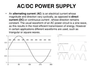
Explore block diagrams, equivalent circuits, transfer characteristics, and waveforms of different rectifier circuits like half-wave, full-wave, and bridge rectifiers in DC power supplies. Learn about limiting circuits and modeling diodes.

E N D
Rectifier Circuit (a) Rectifier circuit. (b) Input waveform. (c) Equivalent circuit when (d) Equivalent circuit when v1 0 (e) Output waveform.
(a) Half-wave rectifier. (b) Equivalent circuit of the half-wave rectifier with the diode replaced with its battery-plus-resistance model. (c) transfer characteristic of the rectifier circuit. (d) Input and output waveforms, assuming that rD R.
Full-wave rectifier utilizing a transformer with a center-tapped secondary winding. (a) Circuit. (b) Transfer characteristic assuming a constant-voltage-drop model for the diodes. (c) Input and output waveforms.
Fig.3.39 The bridge rectifier: (a) circuit and (b) input and output waveforms.
Voltage and current waveforms in the peak rectifier circuit with CR T. The diode is assumed ideal.