Download
1 / 59
600 likes | 868 Vues
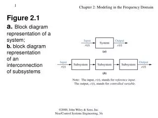
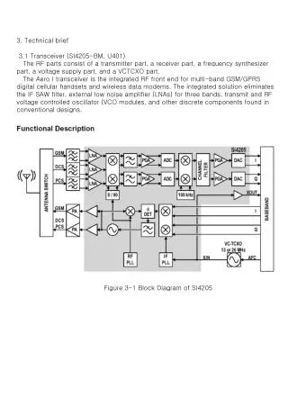
3. Technical brief 3.1 Transceiver (SI4205-BM, U401) The RF parts consist of a transmitter part, a receiver part, a frequency synthesizer part, a voltage supply part, and a VCTCXO part.

E N D
3. Technical brief 3.1 Transceiver (SI4205-BM, U401) The RF parts consist of a transmitter part, a receiver part, a frequency synthesizer part, a voltage supply part, and a VCTCXO part. The Aero I transceiver is the integrated RF front end for multi-band GSM/GPRS digital cellular handsets and wireless data modems. The integrated solution eliminates the IF SAW filter, external low noise amplifier (LNAs) for three bands, transmit and RF voltage controlled oscillator (VCO modules, and other discrete components found in conventional designs. Figure 3-1 Block Diagram of SI4205
(1) Receiver part The Aero I transceiver uses a low-IF receiver architecture which allows for the on chip integration of the channel selection filters, eliminating the external RF image reject filters and the IF SAW filter required in conventional superheterodyne architectures. A. RF front end RF front end consists of Antenna Switch(FL400), two SAW Filters(FL401, FL402) and dual band LNAs integrated in transceiver (U401). The Received RF signals(GSM 925MHz ~ 960MHz, DCS 1805MHz ~ 1880MHz) are fed into the antenna or Mobile switch. The Antenna Switch(FL400) is used to control the Rx and Tx paths. And, the input signals VC1 and VC2 of a FL400 are directly connected to baseband controller to switch either Tx or Rx path on. The logic and current is given below Table 3-1. Three differential-input LNAs are integrated in SI4205. The GSM input supports the GSM 850 (869-849 MHz) or E-GSM 900 (925-960MHz) bands. The DCS input supports the DCS 1800 (1805-1880 MHz) band. The PCS input supports the PCS 1900 (1930-1990 MHz) band. The LNA inputs are matched to the 150Ω balanced output SAW filters through external LC matching networks. The LNA gain is controlled with the LNAG[1:0] and LNAC[1:0] bits in register 05h (Figure 3-2). Table 3-1 The Logic and current DCS TX GSM TX
Figure 3-2 Block Diagram of Receiver part of SI4205 B. Intermediate frequency (IF) and Demodulation A quadrature image-reject mixer downconverts the RF signal to a 100KHz intermediate frequency (IF) with the RFLO from the frequency synthesizer. The RFLO frequency is between 1737.8 to 1989.9 MHz, and is internally divided by 2 for GSM 850 and E-GSM 900 modes. The mixer output is amplified with an analog programmable gain amplifier (PGA), which is controlled with the AGAIN[2:0] bits in register 05h (Figure3-2). The quadrature IF signal is digitized with high resolution A/D converters (ADCs). The ADC output is downconverted to baseband with a digital 100KHz quadrature LO signal. Digital decimation and IIR filters perform channel selection to remove blocking and reference interference signals. The selectivity setting (CSEL=0) or a low selectivity setting (CSEL=1). The low selectivity filter has a flatter group channelization filter is in the baseband chip. After channel selection, the digital output is scaled with a digital PGA, which is controlled with the DGAIN [5:0] bits in register 05h. The amplified digital output signal go through with DACs that drive a differential analog signal onto the RXIP,RXIN,RXQP and RXQN pins to interface to standard analog ADC input baseband ICs. No special processing is required in the baseband for offset compensation or extended dynamic range. Compared to a direct-conversion architecture, the low-IF architecture has a much greater degree of immunity to dc offsets that can arise from RF local oscillator(RFLO) self-mixing, 2nd order distortion of blockers, and device 1/f noise.
(2) Transmitter part The transmit (Tx) section consists of an I/Q baseband upconverter, and offset phase-locked loop (OPLL) and two output buffers that can drive external power amplifiers (PA), one for the GSM 850 (824-849 MHz) and E-GSM 900 (880-915 MHz) bands and one for the DCS 1800 (1710-1785 MHz) and PCS 1900 (1850-1910MHz) bands. A. IF Modulator The baseband converter(BBC) within the GSM chipset generates I and Q baseband signals for the Transmit vector modulator. The modulator provides more than 40dBc of carrier and unwanted sideband rejection and produces a GMSK modulated signal. The baseband software is able to cancel out differential DC offsets in the I/Q baseband signals caused by imperfections in the D/A converters. The Tx-Modulator implements a quadrature modulator. A quadrature mixer upconverts the differential in-phase (TXIP, TXIN) and quadrature (TXQP, TXQN) signals with the IFLO to generate a SSB IF signal that is filtered and used as the reference input to the OPLL. The IFLO frequency is generated between 766 and 896 MHz and internally divided by 2 to generate the quadrature LO signals for the quadrature modulator, resulting in an IF between 383 and 448 MHz. For the E-GSM 900 band, two different IFLO frequencies are required for spur management. Therefore, the IF PLL must be programmed per channel in the E-GSM 900 band. Figure 3-3 Block Diagram of Transmitter part of SI4205
B. OPLL The OPLL consists of a feedback mixer, a phase detector, a loop filter, and a fully integrated TXVCO. The TXVCO is centered between the DCS 1800 and PCS 1900 bands, and its output is divided by 2 for the GSM 850 and E-GSM 900 bands. The RFLO frequency is generated between 1272 and 1483 MHz. To allow a single VCO to be used for the RFLO, high-side injection is used for the GSM 850 and E-GSM 900 bands, and low-side injection is used for the DCS 1800 and PCS 1900 bands. The I and Q signals are automatically swapped when switching bands. Additionally, the SWAP bit in register 03h can be used to manually exchange the I and Q signals. Low-pass filters before the OPLL phase detector reduce the harmonic content of the quadrature modulator and feedback mixer outputs. The cutoff frequency of the filters is programmable with the FIF[3:0] bits in register 04h (Figure 3-3), and should be set to the recommended settings detailed in the register description.
(3) Frequency Synthesizer The Aero I transceiver integrates two complete PLLs including VCOs, varactors, resonators, loop filters, reference and VCO dividers, and phase detectors. The RF PLL uses two multiplexed VCOs. The RF1 VCO is used for receive mode, and the RF2 VCO is used for transmit mode. The IF PLL is used only during transmit mode. All VCO tuning inductors are also integrated. The IF and RF output frequencies are set by programming the N-Divider registers, NRF1, NRF2 and NIF. Programming the N-Divider register for either RF1 or RF2 automatically selects the proper VCO. The output frequency of each PLL is as follows: fout = N x f The DIV2 bit in register 31h controls a programmable divider at the XIN pin to allow either a 13 or 26 MHz reference frequency. For receive mode, the RF1 PLL phase detector update rate (fφ) should be programmed fφ= 100 kHz for DCS 1800 or PCS 1900 bands, and fφ= 200 kHz for GSM 850 and E-GSM 900 bands. For transmit mode, the RF2 and IF PLL phase detector update rates are always fφ=200 kHz. Figure 3-4 Block Diagram of Frequency Synthesizer part of SI4205
3.2 Power Amplifier Module (RF3133, U400) The RF3133 is a high-power, high-efficiency power amplifier module with integrated power control. The device is self-contained with 50 input and output terminals. The power control function is also incorporated, eliminating the need for directional couplers, detector diodes, power control ASICs and other power control circuitry; this allows the module to be driven directly from the DAC output. The device is designed for use as the final RF amplifier in GSM 850, E-GSM 900, DCS and PCS handheld digital cellular equipment and other applications in the 824-849 MHz, 880-915 MHz, 1710-1785 MHz, and 1850-1910 MHz bands. On-board power control provides over 37 dB of control range with an analog voltage input (TX_RAMP); and, power down with a logic “low” for standby operation (TX_ENABLE). External control (BAND_SELECT) is used to select the GSM or DCS band with a logic high or low. A logic low enables the GSM band whereas a logic high enables the DCS band. Figure 3-5 Functional Block Diagram of RF3133
3.3 13 MHz Clock The 13 MHz clock(X400) consists of a TCXO(Temperature Compensated Crystal Oscillator) which oscillates at a frequency of 13 MHz. It is used within the Si4205, analog base band chipset (U101, AD6521), digital base band chipset (U102, AD6525), and MIDI (U200) chipset. Figure 3-6 VCTCXO circuit diagram 3.4 Power Supplies for RF Circuits Two regulators are used for RF circuits. One is MIC5255 (U402), and the other is one port of ADP3522 (U301). MIC5255 (U402) supplies power to transceiver (SI4205, U401). One port of ADP3522 supplies power to VCTCXO (X400). Main power (VBAT) from battery is used for PAM (RF3133, U400) because PAM requires high power. Table 3-2 Power suppliers for RF circuits. Supplier Voltage Powers enabled signal U402 2.85 V U401 RF_EN U301 2.75 V X400 Battery 3.4 ~ 4.2 V U400 Figure 3-7 U402 circuit diagram
3.5 Digital Main Processor (AD6525, U100) (1) Architecture Overview Figure 3-8 Block Diagram of the AD6525 Internal Architecture The internal architecture of AD6525 is shown in Figure 3-8. AD6525 regroups three main subsystems connected together through a dynamic and flexible communication bys network. It also includes onboard system RAM (SRAM) and interfaces with external Flash Memory, Baseband converter functions, and terminal functions like MMI, SIM and Universal System Connector (USC). The Digital Signal Processing (DSP) subsystem primarily hosts all the speech processing, channel equalization and channel codec functions. The code used to implement such functions can be stored in external Flash Memory and dynamically downloaded on demand into the DSP’s program RAM and Instruction Cache.
The microcontroller subsystem supports all the GSM terminal software, including the layer 1, 2 and 3 of the GSM protocol stack, the MMI, and applications software such as data services, test and maintenance. It is tightly associated with on-chip system SRAM and also includes boot ROM memory with a small dedicated routine to facilitate the initialization of the external Flash Memory via code download using the on-chip serial interface to the external Flash Memory interface. The peripheral subsystem is composed of system peripherals such as interrupt controller, real time clock, watch dog timer, power management and a timing and control module. It also includes peripheral interfaces to the terminal functions: keyboard, battery supervision, radio and display. Both the DSP and the MCU can access the peripheral subsystem via the peripheral bus (PBUS). For program and data storage, both the MCU subsystem and the DSP subsystem can access the on chip system SRAM and external memory such Flash Memory. The access to the SRAM module is made through the RAM Bus (RBUS) under the control of the bus arbitration logic. Similarly, access to the Flash Memory is through the parallel External Bus (EBUS).
Figure 3-9 Example of System Interconnection of AD6525 External Interfaces
(2) Interconnection with external devices A. RTC Block Interface Countered by external crystal oscillator (MC-146, X100). The X-tal oscillates 32.768 KHz. B. LCD Module Interface Controlled by LCD_CS, LCD_RES, ADD1, WR, DATA[0:15], LCD_DIM, and LCD_ID. Table 3-3 LCD module interface Description LCD driver chip enable. LCD driver IC has own CS pin LCD_CS LCD_RES This pin resets LCD module. This pin determines whether the data to LCD module are display data or control data. ADD1 can select 16 bit parallel bus. ADD1 is also used to address flash memory. ADD1 Write control. WR Parallel data lines. Color LCD driver chip uses the 16 bit data interface. DATA[0:15] Control signal for white LED(LCD backlight) driver IC. LCD_DIM Reserved for future use. LCD_ID C. RF Interface The AD6525 control RF parts through RF_EN, ANT_SW1/2, PA_EN, PA_BAND, PDNB, S_EN, S_DATA, AND S_CLK.
Table 3-4 RF interface Description GPO Signal Name RF Enable / Disable 4 RF_EN 9 ANT_SW1 Antenna Switch Band Select Antenna Switch Band Select 11 ANT_SW2 PAM Enable / Disable 16 PA_EN PAM Band Select 17 PA_BAND Power Down Input 18 PDNB Serial Enable Input 19 S_EN Serial Data Input 20 S_DATA Serial Clock Input 21 S_CLK D. SIM Interface The AD6525 check status periodically in call mode if SIM card is inserted or not, but the AD6525 don't check in deep sleep mode. Interface signals are SIM_DATAOP, SIM_CLK, SIM_RST, SIM_EN Table 3-5 SIM interface Description This pin receives and sends data to SIM card. This model support 3.0 volt interface SIM card. SIM_DATAOP SIM_CLK Clock 3.25 MHz frequency. SIM_RST Reset SIM Block Enable SIM Block SIM_EN E. Key Interface Key Interface includes 5 column (KEYCOL[0:4]) and 5 row (KEYROW[0:4]). AD6525 detects key press by interrupt.
F. ADP3522(PMIC, U301) Interface There are 4 signals for PMIC (power management IC) interface. Table 3-6 PMIC interface Description The pin is activated when charger is inserted. CHRDET CHG_EN Enable charging EOC The pin is activated by PMIC when VBAT reaches 4.2V. GATE_EN Control signal from AD6525 to charge NiMH battery. Not used.
3.6 Analog Main Processor (AD6521, U101) (1) Block Diagram Figure 3-10 Functional Block Diagram of AD6521
(2) BB Transmit Section This section generates in-phase and quadrature BB modulated GMSK signals (BT = 0.3) in accordance with GSM 05.05 Phase 2 specifications. The transmit channel consists of a digital GMSK modulator, a matched pair of 10-bit DACs and a matched pair of reconstruction filter. There are TXIP, TXIN, TXQP, TXQN, and RAMPDAC. (3) BB Receiver Section This section consists of two identical ADC channels that process baseband in-phase(I) and quadrature(Q) input signals. Each channel consists of a coarse switched capacitor input filter, followed by a high-order sigma-delta modulator and a lowpass digital filter. There are RXIP, RXIN, RXQP, and RXQN. (4) Auxiliary Section This section contains two auxiliary DACs(AFC DAC, IDAC) for system control. This section also contains AUX ADC and Voltage Reference AUX ADC : 6 channel 10 bits AFC DAC : 13 bits IDAC : 10 bits (5) Voiceband Section Receive audio signal from MIC. The phones use differential configuration. Send audio signal to Receiver. The phones use differential configuration. It interconnects external devices such as main microphone, main receiver, ear-phone and Hands free kit through the VINNORP, VINNORN, VOUTNORP, VOUTNORN, VINAUXP, VINAUXN, VOUTAUXP, and VOUTAUXN VINNORP, VINNORN: Main MIC positive/negative terminal. VOUTNORP, VOUTNORN: Main Receiver positive/negative terminal. VINAUXP, VINAUXN: Hands free kit microphone positive/negative terminal. VOUTAUXP, VOUTAUXON: Hands free kit speaker positive/negative terminal.
3.7 Power Management IC (ADP3522, U301) Block Diagram Figure 3-12 Block Diagram of ADP3522. Table 3-7 LDOs of ADP3522.
Power on sequence If a battery is inserted, the battery powers the 6 LDOs. Then if PWRONKEY is detected, the LDOs output turn on. REFOUT is also enabled, Reset signal is generated and send to the AD6525. LDO block There are 6 LDOs in the ADP3522. Charging Process 1. Check charger is inserted or not. 2. If ADP3522 detects that Charger is inserted, the CC-CV charging starts. 3. Exception: When battery voltage is lower than 3.2V, the trickle charge (low current charge mode) starts firstly. After the battery voltage reaches to 3.2V, the CC-CV charging starts. Battery charging block It can be used to charge Lithium Ion and/or Nickel Metal Hydride batteries. The phones use Li-Ion battery only. Charger initialization, trickle charging, and constant current charging are implemented in hardware. Pins used for charging CHGDET : Interrupt to AD6525 when charger is plugged. CHG_EN : Control signal from AD6525 to charge battery. EOC : Interrupt to AD6525 when battery is fully charged. GATE_EN : Control signal from AD6525 to charge NiMH battery. But, not used. TA (Travel Adaptor) Input voltage : AC 110V ~ 240V, 50~60Hz Output voltage : DC 5.2V(±0.2 V) Output current : Max 800mA Battery Li-ion battery : Max 4.2V, Nom 3.7V Standard battery : Capacity - 950mAh, Li-ion
3.8 Memory (U300) The memory is consists of 128Mbit Nor Flash Memory and 32Mbit Pseudo SRAM. It has 16 bit parallel data bus and 22 bit address. Software, RF calibration data, audio parameters and battery calibration data are stored in the Flash memory. Figure 3-13 Block Diagram of Memory. Figure 3-8 Pin Description of U300.
3.9 LCD and LCD Backlight (1) LCD Features Display Mode : Transmissive 65K Color STN LCD Color Depth : 32(Red) * 64(Green) * 32(Blue) = 65K Color Resolution : 128 * RGB * 128 dots for Color display Interface : 80-series MPU interface Data bus : 16 bit Parallel interface Duty ratio : 1/96 Duty for Color display Viewing Direction : 12 o'clock LCD Driver : S6B33B2 by SEC Display RAM capacity : 132 x 16 x 162 = 342.144K bits for Color display Control Signal is explained in Table 3-3. (2) LCD Backlight For LCD backlight illumination, there is a driver (U600) which is driven by LCD_DIM signal from AD6525. Power for the driver is supplied by VBAT. Figure 3-14 Circuit Diagram of Driver IC for LCD backlight.
3.10 Keypad Switches and Key Backlight Illumination (1) Keypad Switches The key switches are metal domes, which make contact between two concentric pads on the keypad layer of the PCB when pressed. There are 21 switches (KB500-KB522), connected in a matrix of 5 rows by 5 columns, as shown in Figure, except for the power switch (KB500), which is connected independently. Functions, the row and column lines of the keypad are connected to ports of AD6525. The columns are outputs, while the rows are inputs and have pull-up resistors built in. When a key is pressed, the corresponding row and column are connected together, causing the row input to go low and generate an interrupt. The columns/rows are then scanned by AD6525 to identify the pressed key. Figure 3-15 Circuit Diagram of Keypad Switches.
(2) Key Backlight Illumination There are 6 blue LEDs for key backlight illumination which are driven by KEY_BACKLIGHT signal from AD6525. Figure 3-16 Circuit Diagram of Key backlight illumination
3.11 Microphone The microphone is placed to the front cover and is connected to main PCB. The audio signal is passed to VINNORP and VINNORN pins of AD6525. The voltage supply 2V55_VAN is output from ADP3522, and is a bias voltage for the VINNORP. The VINNORP and VINNORN signals are A/D converted by the Voiceband ADC part of AD6521. The digitized speech is then passed to the DSP section of AD6525 for processing (coding, interleaving etc). Figure 3-17 Circuit Diagram of Microphone.
3.12 Dual Mode Speaker and MIDI IC (1) Dual Mode Speaker There is a control signal (SPK_RCV_EN) which is for enabling receiver or speaker because one dual mode speaker is used for both receiver and speaker. The signal is produced by AD6525 and controls the analog switch (U201). The dual mode speaker is placed in the front cover and contacted to PCB. A. Receiver Operation The dual mode speaker is driven by VOUTNORP and VOUTNORN of AD6521 through a analog switch (U201) when it is used for receiver. The gain is controlled by the PGA in AD6521. B. Speaker Operation The dual mode speaker is driven by SPOUT1 and SPOUT2 of YMU759B (U200) through the analog switch (U201) when it is used for loud speaker. Figure 3-18 Circuit Diagram of Dual Mode Speaker.
(2) MIDI IC (YMU759B, U200) The phone uses melody IC which makes the robust joyful melody sounds. 6 signals (MIDI_RST, ADD0, RD, MIDI_CS, WR, MIDI_INT) from AD6525 are used to control the melody IC. Melody data (DATA[8:15]) is transferred to melody IC and played by the dual mode speaker. External 3.3V LDO (U202) is used for the MIDI chip because the maximum output current of analog amplifier in melody IC is 300mA. Figure 3-19 Circuit Diagram of MIDI-IC and external LDO.
3.13 Headset Jack Interface 3-pole type ear-mic jack which has three electrodes such as Receiver+, Mic+, and GND. This type usually supports only single-ended configuration (VOUTAUXP for headset speaker and VINAUXP for headset mic) in the audio path. There are two control signals for jack interface. One is JACK_DETECT which is for detecting the headset jack and the other is HOOK_DETECT which is enabled when hook of the headset is pressed. The pins (JACK_DETECT and HOOK_DETECT) interfaces with AD6525. Figure 3-20 Circuit Diagram of Headset Interface.
4. Trouble Shooting 4.1 RF Components SW 400 FL400 FL401 FL402 U402 U401 U400 X400 Figure 4-1 Table 4-1 Reference Description Reference Description Mobile Switch Power Amplifier Module SW400 U400 FL400 Antenna Switch U401 Transceiver LDO FL401 Saw Filter for GSM U402 FL402 Saw Filter for DCS X400 VCTCXO
START HP8922 : Test mode 62 CH, 7 level setting (TCH) 62 CH, -60dBm setting (BCCH) Spectrum analyzer setting Oscilloscope setting 1. Check Regulator Circuit 2. Check VCTCXO Circuit 4. Check Ant SW & Mobile SW 6. Check RX IQ 3. Check Control Signal 5. Check Saw Filter Circuit 4.2 RX Trouble 4 5 1 3 2 6 Figure 4-2
Changing the Board Check Pin 3. Replace U402 No Check Pin 5. Yes RF 2.85V O.K? Pin3. High ? No Yes Regulator Circuit is OK See next Page to check VCTCXO 4.2.1 Checking Regulator Circuit U402.5 U402.3 Figure 4-3 VRF Graph 4-1
Check Pin 3. Refer to Graph 4-2 Yes 13 MHz O.K? Yes Check Pin 4. Refer to Graph 4-3 2.75V OK? No Check U301, PMIC Changing X400 No VCTCXO Circuit is OK See next Page to check ANT SW & Mobile SW Graph 4-2 4.2.2 Checking VCTCXO Circuit Figure 4-4 X400.3 X400.4 Graph 4-3
Download the SW Download the SW No Check TP 401. Level is High? Check TP 402, 403, 404. Check if there is Any Major Difference Refer to Graph 4-5 No Similar? Yes Yes Control Signal is OK See next Page to check ANT SW & Mobile SW 4.2.3 Checking PLL Control Signal S_DATA (TP404) S_CLK (TP403) S_EN (TP402) PDNB (TP401) Figure 4-5 Graph 4-4 Graph 4-5
No Short No Changing FL400 Changing SW400 No Yes VC1 :Low VC2 :Low Changing the Board. Ant SW & Mobile SW is OK See next Page to check Rx IQ Signal 4.2.4 Checking Antenna Switch & Mobile Switch SW400.ANT SW400.RF FL400.10 FL400.1 L405 (VC1) L404 (VC2) Figure 4-6 For these 2 test case, No Call connection is needed Check SW400 Pin ANT,RF with RF Cable connected. Changing SW400 Open Yes Check SW400 Pin ANT,RF with No RF Cable Connected • Check L404, L405 • Check whether Ant SW • Set as RX mode • Refer to Table 4-2 Yes Check RF Level of FL400.10 (for GSM) & FL400.1 (for DCS) Pin10 : ~ -62dBm No Pin 1 : ~ -63dBm Table 4-2 Yes ANT SW VC1 VC2 DCS TX 0 1 EGSM TX 1 0 EGSM, DCS RX 0 0 For this RF Level test case, RX Stand alone Mode is needed refer to chapter 11
Changing FL401 for GSM, FL402 for DCS Changing L402, C420 for GSM L403, C425 for DCS No Saw Filter is OK See next Page to check Rx IQ Signal 4.2.5 Checking SAW Filter FL401 FL402 Figure 4-7 Check RF Level of Saw Filter Input For GSM : FL401.1 Changing C422 for GSM No FL401.1 : ~ -61dBm Check the parts are well Soldered For GSM : C422 Yes Check RF Level of Saw Filter Input For GSM : FL401.3 For DCS : FL402.3 No FL401.3: ~ -64dBm Soldering is OK? Yes FL402.3: ~ -64dBm Check the parts are well Soldered For GSM : L402,C420 For DCS : L403, C425 Yes For the test, RX Stand alone Mode is needed. Refer to chapter 11
Replace U401 4.2.6 Checking RX IQ C417,C419 Figure 4-8 Check C417, C419. Check if there is Any Major Difference Refer to Graph 4-6 No Similar? Yes Redownload the Software And calibrate Graph 4-6
START HP8922 : Test mode 62 CH, 7 level setting (TCH) 62 CH, -60dBm setting (BCCH) Spectrum analyzer setting Oscilloscope setting 1. Check Regulator Circuit 2. Check VCTCXO Circuit 6. Check Ant SW & Mobile SW 4. Check TX IQ 3. Check Control Signals 5. Check PAM Control Signal 4.3 TX Trouble 6 1 3 5 2 4 Figure 4-9
Changing the Board Replace U402 Yes Regulator Circuit is OK See next Page to check VCTCXO 4.3.1 Checking Regulator Circuit U402.5 U402.3 Figure 4-10 Check Pin 3. No Check Pin 5. RF 2.85V O.K? Pin3. High ? No Yes VRF Graph 4-7
Check Pin 3. Refer to Graph 4-8 Yes 13 MHz O.K? Yes Check Pin 4. Refer to Graph 4-9 2.75V OK? No Check U301, PMIC Changing X400 No VCTCXO Circuit is OK See next Page to check ANT SW & Mobile SW Graph 4-8 4.3.2 Checking VCTCXO Circuit Figure 4-11 X400.3 X400.4 Graph 4-9
Download the SW Download the SW No Check TP 401. Level is High? Check TP 402, 403, 404. Check if there is Any Major Difference Refer to Graph 4-11 No Similar? Yes Yes Control Signal is OK See next Page to check ANT SW & Mobile SW 4.3.3 Checking PLL Control Signal S_DATA (TP404) S_CLK (TP403) S_EN (TP402) PDNB (TP401) Figure 4-12 Graph 4-10 Graph 4-11
Replace U401 4.3.4 Checking TX IQ C421,C424 Figure 4-13 Check C421, C424. Check if there is Any Major Difference Refer to Graph 4-12 No Similar? Yes Redownload the Software And calibrate Graph 4-12
Check TX_RAMP and PA_EN Check if there is Any Major Difference or not Refer to Graph 4-13 No Similar? Yes Go to Next Step Download S/W 4.3.5 Checking PAM Control Signal TX_RAMP (R401) PA_EN (R402) Figure 4-14 Graph 4-13
Short Changing board Changing SW400 Yes 4.3.6 Checking Antenna Switch & Mobile Switch SW400.ANT SW400.RF FL400.5 FL400.3 L405 (VC1) L404 (VC2) Figure 4-15 For the test, TX Stand alone Mode is needed. Refer to chapter 11 (PL=7 for GSM, PL=2 for DCS) • Check L405, L404 • Check whether Ant SW • Set as TX mode • Refer to Graph 4-14,15 • Refer to Table 4-3 No Check VC1, VC2 Yes Check RF Level of FL400 Pin 5 (for GSM) & Pin 3 (for DCS) Go to 4.3.5 Checking PAM control signal Pin5 : ~29.5dBm No Pin 3 : ~26.5dBm Table 4-3 Yes ANT SW VC1 VC2 Check SW400.ANT, RF with RF Cable connected. Changing SW400 No Open DCS TX 0 1 Yes EGSM TX 1 0 Check SW400.ANT,RF with RF Cable disconnected No EGSM, DCS RX 0 0 END
(VC1) (VC2) (VC1) (VC2) Graph 4-14 DCS TX Graph 4-15 EGSM TX
START No Check Battery Voltage Charge or Change Battery > 3.35V ? Yes Push power-on key and check the level change of U301 Pin 30 No Check the contact of power-key or dome switch. Yes Check the voltage of the following pins at U301 No Pin 21 = 1.8V ? Replace U301 Pin 25 = 2.75V ? Pin 20 = 2.8V ? Pin 3 = 2.0V ? Yes No Logic level at pin 29 of U301 Redownload software = HIGH? Yes THE PHONE WILL POWER ON. 4.4 Power On Trouble SETTING : Connect PIF, and set remote switch off at PIF * Refer to Figure 16
U301.21 1V8_VCORE U301.20 2V8_VMEM U301.25 2V75_VTCXO U301.29 RPWRON U301.30 POWERKEY Figure 4-16 U301.3 2V0_VRTC
4.5 Charging Trouble SETTING : Connect the battery (3.4 ~ 4V) and the charging adaptor(TA) to the phone START No Charging Connector(CN601) Re-solder CN601. well-soldered? Yes No The charging adaptor(TA) is out of order. Voltage at Pin 7 of U301 Change the charging adaptor. = 5.2V? Yes No R300, Q300, D300 well-soldered? Re-solder R300, Q300, D300 . Yes No Voltage across D300 = ~0.3V Replace D300. Yes Voltage across R300 is ~160mV. No Replace R300. Yes No ~0.7< Voltage(Q300) < ~1.3V Replace Q300 Yes No The battery may have the problem. Is the battery charged ? Change the battery and try again. Yes CHARGING WILL OPERATE PROPERLY.
Charging current direction R300 Q300 D300 Figure 4-17
START PIF Power On Reassemble LCD module with LCD connector No Is the connection of LCD module with LCD connector on PCB OK? Yes Not OK Check the soldering Of CN600 Re-solder CN600 OK Check pin9 of U600 is high when backlight are turned on No No Does LCD backlight work properly? Download S/W Yes Replace U600 No Does LCD work properly? Replace LCD module Yes LCD Working!! 4.6 LCD Trouble CN600 Figure 4-18 U600.9 (LCD_DIM) U600 Figure 4-19
R206 U201 R207 R209 START Check the signal level of RCVP & RCVN at R206, R207. Are these voltage is about 1.2V? No No Check the soldering R206 & R207 Replace the Main board. ABB is out of order. Yes Re-soldering R206, R207 Yes No No Check the signal level at R209. Is it almost 0? Check the soldering of U201 Replace U201 Yes Yes Re-soldering U201 No Check the contact state of dual mode speaker. Replace the dual mode speaker The dual mode speaker will work properly. 4.7 Receiver Trouble Figure 4-20
START No No Replace U202 ( Melody IC LDO) Voltage across C235 = 3.3 V? Check the soldering of U202 Yes Yes Re-soldering U202 No No Voltage across C238 = 2.8 V? Replace U302 Check the soldering of U302 Yes Yes Re-soldering U302 No Check the signal level of R234, R236 Replace U200 Yes The voltage of R209 is ~2.8V No No Replace U201 Check the soldering of U201 Yes Re-soldering U201 No Check the state of contact of dual mode speaker Replace speaker Yes Speaker Working!! 4.8 Speaker Trouble SETTING: Connect PIF to the phone, and Power on. Enter The engineering mode, and set “Melody on” at Buzzer of BB test menu