CMOS Transistors
CMOS Transistors. Outline. Qualitative Description of CMOS Transistor g m /I D Design Biasing a transistor Using g m /I D Approach Design Using Cadence. A Crude Metal Oxide Semiconductor (MOS) Device . V2 causes movement of negative charges, thus current. V1 can control the


CMOS Transistors
E N D
Presentation Transcript
Outline • Qualitative Description of CMOS Transistor • gm/ID Design • Biasing a transistor Using gm/ID Approach • Design Using Cadence
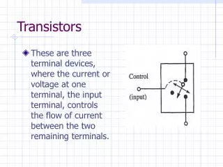
A Crude Metal Oxide Semiconductor (MOS) Device V2 causes movement of negative charges, thus current. V1 can control the resistivity of the channel. Positive charge attract negative charges to interface between insulator and silicon. A conductive path is created If the density of electrons is sufficiently high. Q=CV. P-Type Silicon is slightly conductive. The gate draws no current!
An Improved MOS Transistor (provide electrons) (drain electrons) n+ diffusion allows electrons move through silicon.
Typical Dimensions of MOSFETs These diode must be reversed biased. tox is made really thin to increase C, therefore, create a strong control of Q by V.
A Closer Look at the Channel Formulation Need to tie substrate to GND to avoid current through PN diode. VTH=300mV to 500 mV (OFF) (ON) Free electrons appear at VG=VTH. Positive charges repel the holes creating a depletion region, a region free of holes.
Channel Resistance As VG increases, the density of electrons increases, the value of channel resistance changes with gate voltage.
Drain Current as a function of Drain Voltage Resistance determined by VG.
Drain Current as a function of Gate Voltage Higher VG leads to a lower channel resistance, therefore larger slope.
Length Dependence The resistance of a conductor is proportional to the length.
Dependence on Oxide Thickness Q=CV C is inversely proportional to 1/tox. Lower Q implies higher channel resitsance.
Width Dependence The resistance of a conductor is inversely proportional to the cross section area. A larger device also has a larger capacitance!
Channel Pinch Off • Q=CV • V=VG-VOXIDE-Silicon • VOXIDE-Silicon can change along the channel! Low VOXIDE-Silicon implies less Q.
VG-VD is sufficiently large to produce a channel VG-VD is NOT sufficiently large to produce a channel No channel Electrons are swept by E to drain. Drain can no longer affect the drain current!
Regions (No Dependence on VDS) No channel
Determination of Region • How do you know whether a transistor is in the linear region or saturation region? • If VDS>(VGS-VTH) and VGS>VTH, then the device is in the saturation region. • If VDS<(VGS-VTH) and VGS>VTH, then the device is in the linear region.
Limited VDS Dependence During Saturation As VDS increase, effective L decreases, therefore, ID increases.
Transconductance • As a voltage-controlled current source, a MOS transistor can be characterized by its transconductance: • It is important to know that
Body Effect The threshold voltage will change when VSB=0!
Experimental Data of Body Effect The threshold voltage will increase when VSB increases.
gm/ID Design Flow Specs Design Equations (Analytical) gm/Id Data Set (Emprical) gm/ID Design Optimization (F. Silveira, JSSC, 1996.) W/L Ratios
Intuition gm gds gm/ID gm/gds 2gm 2gds gm/ID gm/gds 2gm 2gds gm/ID gm/gds
gm/ID Data Set • gm/gds • gm/gmbs • ID/W • Cgd/Cgg • Cgs/Cgg • ….more (F. Silveira, JSSC, 1996.)
Calculation Initially assume that gmro is large! (gm is determined)
gm/gds (50)
Biasing an MOS Transistor Using gm/ID technique Section 7.1 J.Ou Sonoma State Univeristy
Basic Analysis Use 1.2 V (Modified Ex 7.1)
Assumption: VDD=1.2 V Transistor Information: Type: 120 nm Specify VDS Note var1_1 is ‘vsd’ if pmos is used Note var2_1 is ‘vns’ if nmos is used. In this example, is initially unknown, so we will assume that it is 0.0
Interpolation Since the database base can not be so large as to keep all possible values of vds/vsb, we have to interpolate based on existing values, which are available On 0.1 V interval. Current release: need to enter inBias <= the minVar1 and maxVar1. minVar=maxVar-0.1
Browse Database dBrowse2D(25, 'pfet', '15.0u', 'vsd', 0.3, 0.4, 0.353, 'vns', 0.5, 0.6, 0.577, 'vth') Variable name=dBrowse2D(gmoverid, type, length, var1, minVar1, maxVar1,inBias1, var2, minVar2, maxVar2,inBias2, ‘parameter’ ) Valid parameters: gmovergds, gmovergmbs, vth, ft, gmoveridft, idoverw, vod, region, fndbderiv cgdovercgg,cddovercgg, cgsovercgg, csbovercgg, cdbovercgg, ron, vdsat, rseff, rdeff type: nfet, pfet length: {'120n' '180n' '250n' '350n' '600n' '800n' '1.0u' '2.0u' '3.0u' '4.0u' '5.0u' '6.0u' '7.0u' '8.0u' '9.0u' '10.0u' '15.0u' '20.0u'} (text string)
Iteration • Start with • length=‘120nm’ • gmoverid=20 • VDS=VDD/2, VSB=0 • Calculate • vod_1 • vth_ • vgs_1 • vx (gate voltage) • vs (source voltage) • ID • Idoverw • W • RD • Vd • Vds=Vd-Vs
Start Cadence Start Cadence