Download
1 / 13
130 likes | 312 Vues
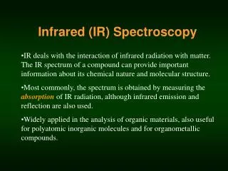
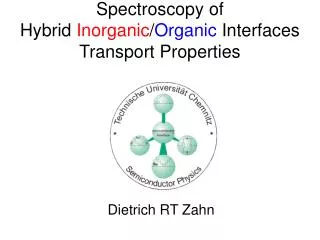
Spectroscopy of Hybrid Inorganic / Organic Interfaces Transport Properties. Dietrich RT Zahn. Metal. I. Organic Interlayer. GaAs(100). V. (v i ) The Overall Device Performance. ( v ) The Metal film. (iv) The Interface between the Organic Molecules and the Metal.

E N D
Spectroscopy of Hybrid Inorganic/Organic InterfacesTransport Properties Dietrich RT Zahn
Metal I Organic Interlayer GaAs(100) V (vi) The Overall Device Performance (v) The Metal film (iv) The Interface between the Organic Molecules and the Metal (iii) The Organic Molecular Film (ii) The Interface between GaAs Substrate and Organic Molecules (i)The GaAs Substrate Surface
Ag/PTCDA/GaAs Ag/GaAs PTCDA modified Ag/GaAs(100) Schottky Contacts • 30 nm PTCDA interlayer. • Reverse bias/Low forward bias • Increase in current ( 1000) • Decrease in barrier height ( -150 meV) • High forward bias • Deviation from pure thermionic emission. 3,4,9,10-Perylenetetracarboxylic dianhydride ( C24H8O6)
IV Characteristics of Ag/PTCDA/GaAs(100) Diodes Low injection region: • Current Iincreaseswith layer thickness d. • Current can be described by thermionic emission. • High injection region: • Current Idecreaseswith layer thickness d. • Space charge effectsgovern the transport behaviour.
I/V Characteristic of organic modified Schottky Contacts • Thermionic emission • Space charge limited current (SCLC) • Series resistance 30 nm PTCDA SCLC in the PTCDA layer (Mott-Gurney) Diode parameters n =1.280.01B,eff =(0.660.01)eV RS =(6.81.0) eff =(1.30.3)10-2 cm2/Vs V= Vbarrier + Vorg+ VR
Effect of Sulfur Treatments on Ag/GaAs(100) Schottky contacts • Difference in barrier height: • in agreement with PES results. • St. Hohenecker et al., J. of Electron. Spectr. and Rel. Phen., 96 (1998) 97. • due to an additional S-induced surface dipole. • T.U. Kampen et al., Surf. Sci. 331-333 (1995) 490; W. Mönch, Europhys. Lett. 27 (1994) 479. Ag/S-GaAs(100) n=1.090.01 B,eff=(0.590.01)eV Ag/GaAs(100) n=1.100.01 B,eff=(0.820.01)eV
IV Characteristics for Ag/PTCDA/S-GaAs(100) • Low injection region: • - Initial decrease in current, then increase • - Saturation above 30 nm. • High injection region: • - Dominated by SCLC
Effective Barrier Height for Ag/PTCDA/GaAs(100) Diodes • Ag/PTCDA/GaAs • B =0.64~0.81 eV • Ag/PTCDA/S-GaAs • B =0.54~0.73 eV The effective barrier height can be tuned by different surface treatments and by the organic modification.
CV Characteristics Ag/PTCDA/GaAs(100) Diodes CO: Capacitance of PTCDA CD: Capacitance of GaAs • Unmodified contact • CD 0.22 nF • 60 nm PTCDA interlayer • Capacity of the organic layer decreases: • C = 0.134 nF CO 0.34 nF • GaAs space charge region is not changed! Frequency: 1MHz Ag/GaAs 3 nm 5 nm 10 nm 15 nm 30 nm 60 nm
IV Characteristics of Ag/PTCDA/GaAs(100) Diodes Low injection region: • Current Iincreaseswith layer thickness d. • Current can be described by thermionic emission. • High injection region: • Current Idecreaseswith layer thickness d. • Space charge effectsgovern the transport behaviour.
IV Characteristics for Ag/PTCDA/S-GaAs(100) • Low injection region: • - Initial decrease in current, then increase • - Saturation above 30 nm. • High injection region: • - Dominated by SCLC
Effective Barrier Height for Ag/PTCDA/GaAs(100) Diodes • Ag/PTCDA/GaAs • B =0.64~0.81 eV • Ag/PTCDA/S-GaAs • B =0.54~0.73 eV The effective barrier height can be tuned by different surface treatments and by the organic modification.
The Influence of Air Exposure on Deep Level of Ag/PTCDA(100ML)/GaAs:S-21 • Assignment: • B - GaAs bulk ET2 • C - PTCDA • D - PTCDA • After air exposure • Dramatic increase of C, D • Increase of trap density • Decrease of effective mobility in PTCDA layer • Change the energy level at the interface