Spatial Distribution Analysis of Superconducting Films using Variable Temperature Scanning Laser Microscopy
10 likes | 91 Vues
Investigating spatial resistive properties in wide superconducting films using VTSLM. Technique measures bolometric response with laser beam. Study reveals non-uniform Tc distribution. Development in coated conductor diagnosis.

Spatial Distribution Analysis of Superconducting Films using Variable Temperature Scanning Laser Microscopy
E N D
Presentation Transcript
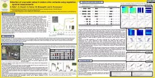
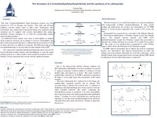
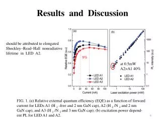
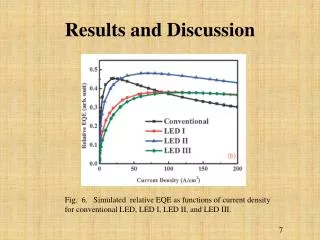
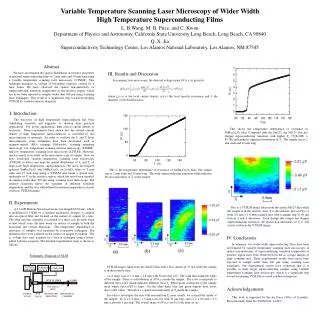
LOCK-IN AMPLIFIER CURRENT SOURCE COMPUTER OPTICAL FIBER LASER FOCUSING OPTIC XYZ STAGE SAMPLE STAGE MECHANICAL CHOPPER MICROSCOPE OBJECTIVE Schematic Diagram of SLM Variable Temperature Scanning Laser Microscopy of Wider Width High Temperature Superconducting Films L. B.Wang, M. B. Price, and C. Kwon Department of Physics and Astronomy, California State University Long Beach, Long Beach, CA 90840 Q. X. Jia Superconductivity Technology Center, Los Alamos National Laboratory, Los Alamos, NM 87545 Abstract We have investigated the spatial distribution of resistive properties in epitaxial superconducting films of 2 mm wide and 10 mm long using a variable temperature scanning laser microscopy (VTSLM). This technique measures ac voltage of bolometric response created by a laser beam. We have observed the spatial non-uniformity of superconducting transition temperature in the resistive region, which has never been reported in samples wider than 300 m using scanning laser techniques. This result is a significant step toward developing VTSLM for coated conductor diagnosis. I. Introduction The discovery of high temperature superconductor has been stimulating scientists and engineers to develop their practical applications. For power applications, high critical current density is necessary. Many experiments have shown that the critical current density of high temperature superconductors is controlled by the microstructure of materials. In order to evaluate the Jc and Tc from microstructure, some techniques have been developed, such as magneto-optical (MO) imaging, Hall-probe, scanning tunneling microscopy, low temperature scanning electron microscopy (LTSEM), and low temperature scanning laser microscopy (LTSLM). However, much research is executed on the micrometer scale of sample. Now we have developed variable temperature scanning laser microscope (VTSLM) to detect and map the spatial distribution of Jc and Tc of large-scale high temperature superconductors. We have investigated epitaxial SmBa2Cu3O7 and NdBa2Cu3O7 on LaAlO3 films of 2 mm wide and 10 mm long using a VTSLM and found a spatial non-uniformity of Tc in the resistive region, which has never been reported in samples wider than 300 m using scanning laser microscope. The resistive transition shows the signature of different transition temperature, and the area with different transition temperature is clearly visible in VTSLM images. II. Experiments A 5.2 mW Helium-Neon laser beam (wavelength 632.8 nm), which is modulated at 1 KHz by a standard mechanical chopper, is coupled into an optical fiber and focused on the surface of sample by a lens. The fiber and lens assembly is fastened to a three-axis movable stage system which scans the laser beam on surface of sample in both the horizontal and vertical directions. The temperature dependence of resistance of samples was measured by four-probe techniques. The platinum wires were soldered on the surface of sample by indium. The ac voltage data were acquired by a lock-in technique using a home-edited Labview program. The detailed experimental setup is shown as follows: III. Results and Discussion In scanning laser microscopy, the detected voltage signal V(x,y) is given by where jb(x,y) is the local current density, (x,y) the local specific resistance, and the diameter of the disturbed area. This shows the temperature dependence of resistance in NdBa2Cu3O7 film. Compared with the Sm123, the Nd123 film has sharper superconducting transition with higher Tc (Tc(R=0W) = 85.7K) indicating no apparent distribution of Tc. The sample size is 2 mm wide and 10 mm long. This is the temperature dependence of resistance of SmBa2Cu3O7 film. The sample size is 2 mm wide and 10 mm long. The wide superconducting transition width indicates the non-uniformity of Tc in the sample. This is a VTSLM image taken from the inside Nd123 film while the sample is in the resistive state. It is the intensity plot of V(x,y) from 2.0 mm 1.6 mm scanned area with scanning step of 40 m both in x and y directions. Even though this sample has sharper superconducting transition, the spatial non-uniformity of Tc is still clearly visible in the VTSLM image. IV. Conclusions In summary, two wider-width superconducting films have been investigated by variable temperature scanning laser microscopy. A spatial non-uniformity of superconducting transition temperature in resistive region have been observed from the ac voltage images of large scanning area. These experimental results have never been reported in sample wider than 300 m using scanning laser techniques. Our experimental results have evidenced that it is possible to study larger superconducting samples using variable temperature scanning laser microscopy, which is a significant step toward developing VTSLM for coated conductor diagnosis. VTSLM images taken from the Sm123 film with a bias current of 15 mA while the sample is in the resistive state. (a) A large scan of 1.2 mm 3.4 mm with 30 m step size. The solid lines mark the edges of the sample. There is a distribution of V(x,y) inside the sample. The color corresponds to different d(x,y)/dT which indicates different local Tc. Red regions correspond to the sample areas where d(x,y)/dT is large. On the other hand, blue and green regions have lower d(x,y)/dT values. This shows a spatial non-uniformity of Tc inside the sample. In order to investigate the area with non-uniform Tc more clearly, we scanned the inside of the sample. (b) is a 1.2 mm 1.8 mm scan size with 30 m step, and (c) is a 0.6 mm 1.0 mm scan with 5 m step. The overall shape of V(x,y) in (b) is the same as (a). Acknowledgements This work is supported by the Air Force Office of Scientific Research under Grant No. F49620-01-1-0493.