Crystal physics
Crystal physics. Crystal physics. The behaviour of material are closely related to their crystal structure. Materials differ from one another in their properties. Material. Non- crystalline or amorphous. Crystalline. CLASSIFICATION OF MATERIALS. Crystalline materials.


Crystal physics
E N D
Presentation Transcript
Crystal physics • The behaviour of material are closely related to their crystal structure. Materials differ from one another in their properties Material Non- crystallineoramorphous Crystalline
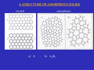
CLASSIFICATION OF MATERIALS Crystalline materials... • atoms pack in periodic, 3D arrays • typical of: -metals -many ceramics -some polymers crystalline SiO2 Si Oxygen Noncrystalline materials... • atoms have no periodic packing • occurs for: -complex structures -rapid cooling "Amorphous" = Noncrystalline noncrystalline SiO2
Important Crystalline material - Atoms are arranged in systematicorregularpatternNon-crystalline material - Atoms are arrangedrandomlyCrystal- 3D solid whichconsistsofperiodicarrangementofatomsCrystal structure - The arrangementofatoms in crystalSpace lattice- The representationofatoms in the crystal in 3D isknownasspacelattice. DefinedasItis an arrayofpoint in space such thateachpoint in spacehas an identicalsorroundingstothatofeveryotherpoint in array.
Space lattice + Basis Crystal structure Crystal structure is formed by adding basis to the lattice points. Basis- It is a single atom or arrangement of atoms which is identical in composition, arrangement and orientation. Unit cell- Smallest geometric figure which is repeated to derive actual crystal structure.
SIMPLE CUBIC STRUCTURE (SC) • Cubic unit cell is 3D repeat unit • Rare (only Po has this structure) • Close-packed directions (directions along which atoms touch each other) are cube edges. • Coordination # = 6 (# nearest neighbors)
Number of Atoms/Unit Cell For atoms in a cubic unit cell: • Atoms in corners are ⅛ within the cell
# of Atoms/Unit Cell For atoms in a cubic unit cell: • Atoms on faces are ½ within the cell
# of Atoms/Unit Cell A face-centered cubic unit cell contains a total of 4 atoms: 1 from the corners, and 3 from the faces.
# of Atoms/Unit Cell For atoms in a cubic unit cell: • Atoms in corners are ⅛ within the cell • Atoms on faces are ½ within the cell • Atoms on edges are ¼ within the cell
ATOMIC PACKING FACTOR • Fill a box with hard spheres - Packing factor = total volume of spheres in box / volume of box - Question: what is the maximum packing factor you can expect? • In crystalline materials: - Atomic packing factor = total volume of atoms in unit cell / volume of unit cell - (as unit cell repeats in space)
ATOMIC PACKING FACTOR SC Volume of atoms in unit cell* Volume of unit cell APF = *assume hard spheres volume a atoms atom 4 R=0.5a unit cell 1 π (0.5a)3 3 APF = close-packed directions a3 volume contains 8 x 1/8 = unit cell 1 atom/unit cell Lattice constant • APF for a simple cubic structure = 0.52
ATOMIC PACKING FACTOR: FCC Close-packed directions: length = 4R = 2 a Unit cell contains: 6 x 1/2 + 8 x 1/8 = 4 atoms/unit cell a atoms volume 4 unit cell 4 π ( 2a/4)3 atom 3 APF = volume a3 unit cell • APF for a body-centered cubic structure = p/(3√2) = 0.74 (best possible packing of identical spheres)
ATOMIC PACKING FACTOR: BCC Close-packed directions: length = 4R = 3 a Unit cell contains: 1 + 8 x 1/8 = 2 atoms/unit cell R a atoms volume 4 unit cell 3a/4)3 2 π ( atom 3 APF = volume a3 unit cell • APF for a body-centered cubic structure = π√3/8 = 0.68
• Assumptions: - To discuss crystalline structures it is useful to consider atoms as being hard spheres with well-defined radii. In this hard-sphere model, the shortest distance between two like atoms is one diameter of the hard sphere.
First, each corner atom is shared among six unit cells. Second, the atoms located in the center of the top and bottom planes belong to only two unit cells. Third, there are three independent atoms in the center of this structure
HEXAGONAL CLOSE-PACKED STRUCTURE (HCP) Ideally, c/a = 1.633 for close packing However, in most metals, c/a ratio deviates from this value
Diamond Structure The diamond lattice consists of two interpenetrating face-centered bravais lattices. There are eight atom in the structure of diamond. Each atom bonds covalently to 4 others equally spread about atom in 3d.
Some features It is formed by carbon atoms Every carbon atom is surrounded by four other carbon atoms (CN - 04) situated at the corners of regular tetrahedral by the covalent linkages. The diamond cubic structure is a combination of two interpenetrating FCC sub lattices displaced along the body diagonal of the cubic cell by 1/4th length of that diagonal. Thus the origins of two FCC sub lattices lie at (0, 0, 0) and (1/4, 1/4,1/4) In diamond cubic unit cell there are 8 corner atoms, 6 face centeredatoms and four other atoms
Diamond Structure a Z No. of atoms present in a 2r XY2 = XW2 + WY2 diamond cubic unit cell is 1+3+4=8 a/4 X 2 2 a Y 2 2 ⎞ ⎛ a ⎞ a/4 ⎛ a ⎛ a ⎞ + ⎟ ⎜ ⎟ ⎜ a/4 +⎜ ⎟ 4 4 ⎝ ⎠ ⎝ ⎠ W 8 ⎝ 4 ⎠ XZ2 = XY2 + YZ2
Diamond Structure Atomic packing factor (APF) But XZ = 2r 2 v 3a APF = ∴(2r)2 = V 16 4 3 2 3a 8 × πr v = = 4r2 3 16 3 4 ⎛ 3a ⎞ 2 3a i.e. v = 8 × π⎜ ⎟ r2= ⎜ ⎟ 3 8 ⎝ ⎠ 64 3 a ∴Atomic radius r = 3 8 × 4π × 3 3 a = 8 APF 3 3 3 × 8 × a APF = π 3 = 0.34 16 Thus it is a loosely packed structure.
COMPARISON OF CRYSTAL STRUCTURES close packed directions Crystal structure coordination # packing factor • Simple Cubic (SC) 6 0.52 cube edges • Body Centered Cubic (BCC) 8 0.68 body diagonal • Face Centered Cubic (FCC) 12 0.74 face diagonal • Hexagonal Close Pack (HCP) 12 0.74 hexagonal side • Diamond (FCC) 12 0.34 face diagonal
Lattice parameter of unit cellA unit cell can be constructed when we know distance between the two lattice points along three direction and angle between themThe intercept made by edges of the unit cell along x, y and Z direction and interfacial angles are the lattice parameter of unit cell In this figure, a,b c and the angle α, β and γ is termed as lattice parameter Simple cube is a primitive cell as No. of atoms per unit cell is one BCC and FCC are non primitive. No. of atoms per unit cell is 2 and 4 respectively.
CRYSTAL SYSTEMS AND BRAVAIS LATTICESSeven crystal systems are each described by the shape of the unit cell which can be translated to fill space.Bravaislattices -- fourteen simple and complex lattices within the seven crystal systems.
MILLER INDICES FOR CRYSTALLOGRAPHIC PLANESDefinition: Miller Indices are the reciprocals of the fractional intercepts (with fractions cleared) which the plane makes with the crystallographic x,y,z axes of the three nonparallel edges of the cubic unit cell.
Miller Indices for planes (0,0,1) Z Y (0,3,0) Intercepts → 1 Plane → (100) Family → {100} → 3 X (2,0,0) • Find intercepts along axes → 2 3 1 • Take reciprocal → 1/2 1/3 1 • Convert to smallest integers in the same ratio → 3 2 6 • Enclose in parenthesis → (326)
Ideal crystal- the atomic arrangement is perfectly regular and continous. But in real crystal due to some reason the arrangements of atom is disturbed along a point or along a line or in a region. The disturbance occured in the regular orientation of atoms is called a deffect Defects or imperfections are favoured thermodynamically • Defects in crystals cause distortion in the arrangement of atoms and subsequently can have tremendous effects on properties.
Dimensional Ranges for Different Classes of Defects a. Point defects (zero-dimensional) b. Line defects (single dimensional) c. Surface defects (two dimensional) d. Volume defects (three dimensional)
Point Defects Atomic point defects. Two most common point defects in compounds: 1) Schottky and 2) Frenkel defects.
Schematic depiction of various point defects -when an ion displaced from a regular position to an interstitial position creating a vacancy, the pair of vacancy-interstitial is calledFrenkel defect. Cations are usually smaller and thus displaced easily than anions. Closed packed structures have fewer interstitials and displaced ions than vacancies because additional energy is required to force the atoms into the interstitial positions. - a pair of one cation and one anion can be missing from an ionic crystal, without violating the condition of charge neutrality when the valency of ions is equal. The pair of vacant sites, thus formed, is called Schottky defect. This type of point defect is dominant in alkali halides. These ion-pair vacancies, like single vacancies, facilitate atomic diffusion.
LINE IMPERFECTIONS (1 D defects) The defects, which take place due to dislocation or distortion of atoms along a line, in some direction are called as ‘line defects ’. Line defects are also called dislocations. In the geometric sense, they may be called as‘one dimensional defects’ It may be ruptured at any place Responsible for plastic deformations (slip). Two examples of line defects in nature: -A corn -Lines in a zebra
An edge dislocation is visualized as the end edge (L: dislocation line) of an extra half plane inserted in a perfect crystal •Burgers vector (b): represents the atomic distortion around the dislocation line (L). •Note that b is normal to L
Burgers Vector • Burgers vector (b) defines the slip vector (slip magnitude and slip direction) • •To find Burgers vector, draw burgers circuit around a dislocation. • •The BV is the same along a dislocation line.
Screw dislocations -displacement of atoms in one part of crystal relative to rest. There is a line of atoms about which the crystals planes are twisted to give effect similar to thread Dislocation line
SURFACE IMPERFECTIONS The defects on the surface of material are called surface defects or plane defects • grain boundaries. • tilt boundaries, • twin boundaries • stacking faults
a) Grain boundaries - Internal structures • have different crystalline arrangements or different compositions, is called as inter-phase boundary • 2 to 10 nm layer thick This defect take place generally during solidification
b) Tilt boundaries - Internal structures • have low angle orientation < 10 degrees • The angle or tilt will be tanθ =b/D - where b = Burgers vector and D = the average vertical distance between dislocations
c) Twin boundaries - Internal structures • a mirror reflection of the arrangement on the other side • Occurs in pair, they are called twin boundaries. At one boundary, orientation of atomic arrangement changes. • And at another boundary, it is restored back. The region between the pair of boundaries is called the twinned region.
d) Stacking faults - Internal structures • stacking of atomic planes is not in a proper sequence throughout the crystal • Partial dislocations of row of atoms are the causes - Removal of atoms - intrinsic fault - Adding - extrinsic
Volume imperfections - 3D Presence of a large vacancy or void space, when cluster of atoms are missed is also considered as a volume imperfection. Foreign particle inclusions and non crystalline regions which have the dimensions of the order of 0.20 nm are also called as volume imperfections. Large scale dimensions of even micron-sized aggregates Radiation-induced melanin grains Polystyrene grains
C) Symmetry operations Refers to internal atomic arrangement, inherent property of crystals