Memory
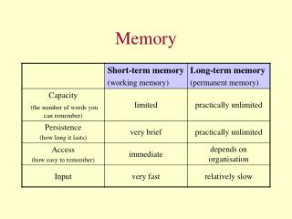
Memory. See: P&H Appendix C.8, C.9. Voting Machine. 3. LED dec. mux. +1. mux. 32. 32. 32. . 32. reg. reg. reg. reg. E. E. E. E. decoder (3-to-8). enc. detect. 3. Register File. Register File N read/write registers Indexed by register number Implementation:

Memory
E N D
Presentation Transcript
Memory See: P&H Appendix C.8, C.9
Voting Machine 3 LED dec mux +1 mux 32 32 32 ... 32 reg reg reg reg E E E E decoder (3-to-8) enc detect 3
Register File • Register File • N read/write registers • Indexed by register number • Implementation: • D flip flops to store bits • Decoder for each write port • Mux for each read port Dual-Read-PortSingle-Write-Port 32 x 32 Register File QA 32 DW 32 QB 32 W RW RA RB 1 5 5 5
Tradeoffs • Register File tradeoffs + Very fast (a few gate delays for both read and write) + Adding extra ports is straightforward – Doesn’t scale
Building Large Memories • Need a shared bus (or shared bit line) • Many FFs/outputs/etc. connected to single wire • Only one output drives the bus at a time
Tri-State Devices Tri-State Buffers E E Vdd D Q D D Q Gnd
Shared Bus D0 S0 D1 S1 D2 S2 D3 S3 D1023 S1023 shared line
SRAM • Static RAM (SRAM) • Essentially just SR Latches + tri-states buffers
SRAM Chip row decoder A21-10 CSR/W column selector, sense amp, and I/O circuits A9-0 Shared Data Bus
SRAM Cell • Typical SRAM Cell bit line word line B B • Each cell stores one bit, and requires 4 – 8 transistors (6 is typical) • Read: • pre-charge B and B to Vdd/2 • pull word line high • cell pulls B or B low, sense amp detects voltage difference • Write: • pull word line high • drive B and B to flip cell
SRAM Modules and Arrays R/W 1M x 4SRAM 1M x 4SRAM 1M x 4SRAM 1M x 4SRAM A21-0 CS msb lsb CS Bank 2 CS Bank 3 CS Bank 4
SRAM Summary • SRAM • A few transistors (~6) per cell • Used for working memory(caches) • But for even higher density…
Dynamic RAM: DRAM • Dynamic-RAM (DRAM) • Data values require constant refresh bit line word line Capacitor Gnd
DRAM vs. SRAM • Single transistor vs. many gates • Denser, cheaper ($30/1GB vs. $30/2MB) • But more complicated, and has analog sensing • Also needs refresh • Read and write back… • …every few milliseconds • Organized in 2D grid, so can do rows at a time • Chip can do refresh internally • Hence… slower and energy inefficient
Memory • Register File tradeoffs + Very fast (a few gate delays for both read and write) + Adding extra ports is straightforward – Expensive, doesn’t scale – Volatile • Volatile Memory alternatives: SRAM, DRAM, … – Slower + Cheaper, and scales well – Volatile Non-Volatile Memory (NV-RAM): Flash, EEPROM, … + Scales well – Limited lifetime; degrades after 100000 to 1M writes
Summary • We now have enough building blocks to build machines that can perform non-trivial computational tasks • Register File: Tens of words of working memory • SRAM: Millions of words of working memory • DRAM: Billions of words of working memory • NVRAM: long term storage (usb fob, solid state disks, BIOS, …)