Bus De-Multiplexing
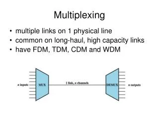
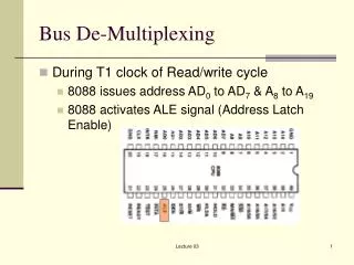
Bus De-Multiplexing. During T1 clock of Read/write cycle 8088 issues address AD 0 to AD 7 & A 8 to A 19 8088 activates ALE signal (Address Latch Enable). 373 Latch. De-multiplexed Bus. GND. OE*. 8088. 373. A 16 – A 19. LE. A 8 – A 15. A 0 – A 7. ALE. GND. 373 Latch. LE. OE*.

Bus De-Multiplexing
E N D
Presentation Transcript
Bus De-Multiplexing • During T1 clock of Read/write cycle • 8088 issues address AD0 to AD7 & A8 to A19 • 8088 activates ALE signal (Address Latch Enable) Lecture 03
373 Latch Lecture 03
De-multiplexed Bus GND OE* 8088 373 A16 – A19 LE A8 – A15 A0 – A7 ALE GND 373 Latch LE OE* AD0 – AD7 D0 – D7 Lecture 03
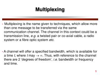
Bus Buffering • Address Lines A0 – A19 have to be buffered • A0 – A7 & A16 – A19 have been buffered by 373 • Logic 0 sinks 32 mA • Logic 1 sources 5.2 mA • A8 – A15 have to be buffered • 74LS244 Octal Buffer used for Buffering Lecture 03
Bus Buffering • Data Lines D0 – D7 have to be buffered • Requires a bi-directional buffer • 74LS245 Octal Bi-directional Buffer • Data Transmit/Receive DT/R* (8088 signal) • Data Bus Enable DEN* (8088 signal) • Enable Pin G (74LS245) • Direction Pin DIR (74LS245) Lecture 03
Bus Buffering • Control Lines RD*, WR* and IO/M* have to be buffered • Buffering introduces time delay Lecture 03
Bus Buffering GND OE* 8088 373 A16 – A19 LE 244 A8 – A15 OE* GND A0 – A7 ALE GND 373 Latch LE OE* DEN* G 245 AD0 – AD7 D0 – D7 DT/R* DIR Lecture 03